
A chip-based test processing method and device

A processing method and chip technology, applied in the field of chip-based test processing and chip-based test processing devices, can solve the problems of inaccurate current, affecting the current of the output port, and being unable to accurately know whether the programming or erasing operation is successful, etc., to achieve Effects of eliminating influence, ensuring accuracy, improving circuit precision and circuit performance

Active Publication Date: 2019-01-01
GIGADEVICE SEMICON (BEIJING) INC
View PDF3 Cites 0 Cited by
  • Summary
  • Abstract
  • Description
  • Claims
  • Application Information

AI Technical Summary

Problems solved by technology

When performing Verify, these bad storage columns and bad replacement columns will affect the current of the output port (such as the SBUS port), making the obtained current inaccurate, which in turn makes it impossible to accurately know whether the programming or erasing operation is successful

Method used


Image

  • A chip-based test processing method and device
  • A chip-based test processing method and device
  • A chip-based test processing method and device

Examples


Embodiment Construction

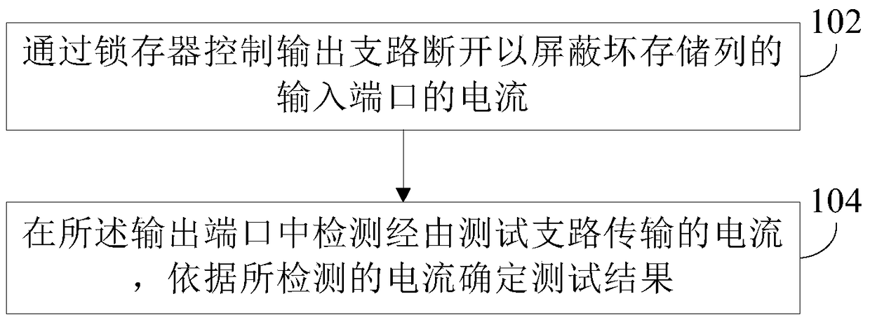
[0041] In order to make the above objects, features and advantages of the present invention more comprehensible, the present invention will be further described in detail below in conjunction with the accompanying drawings and specific embodiments.

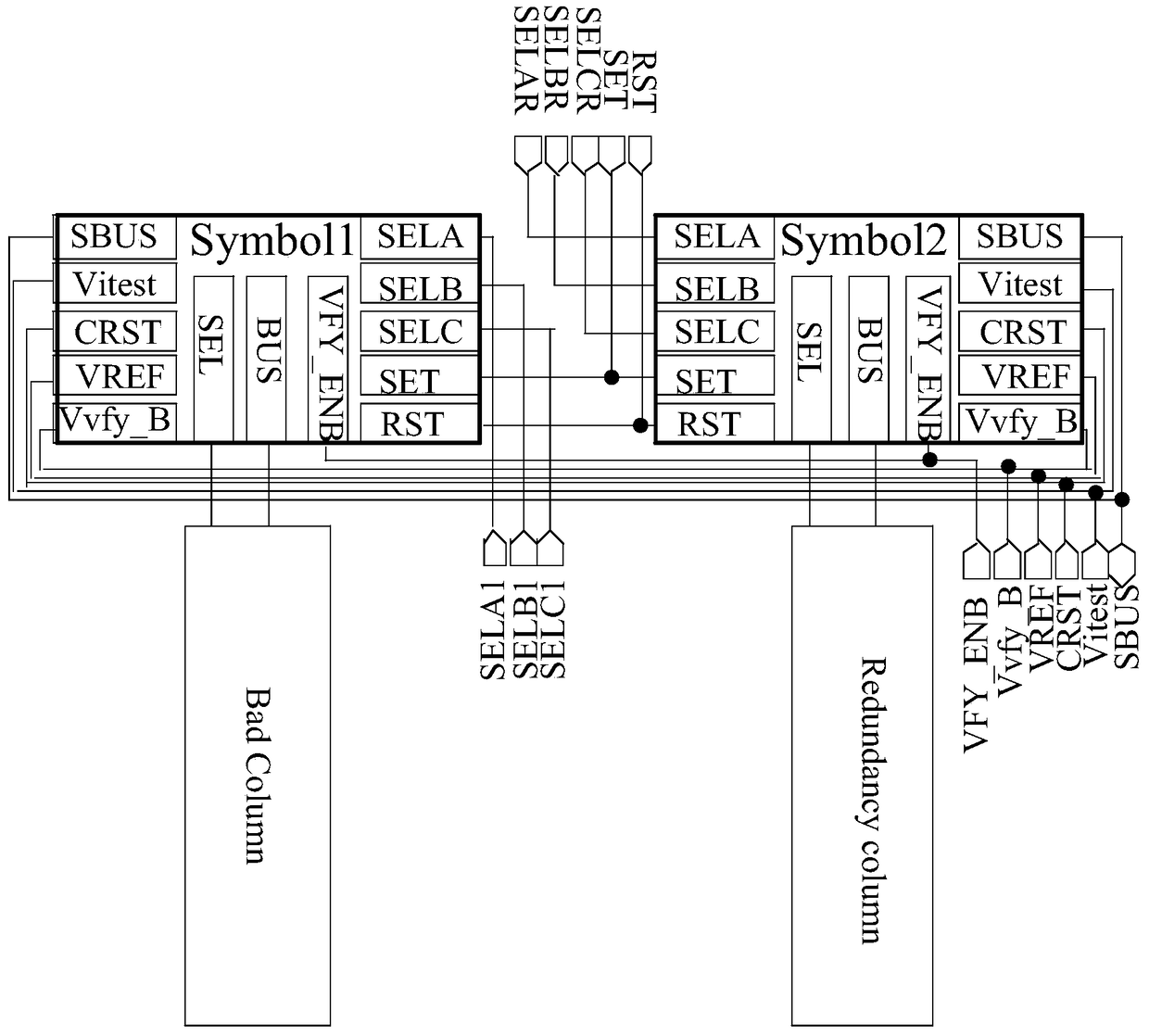
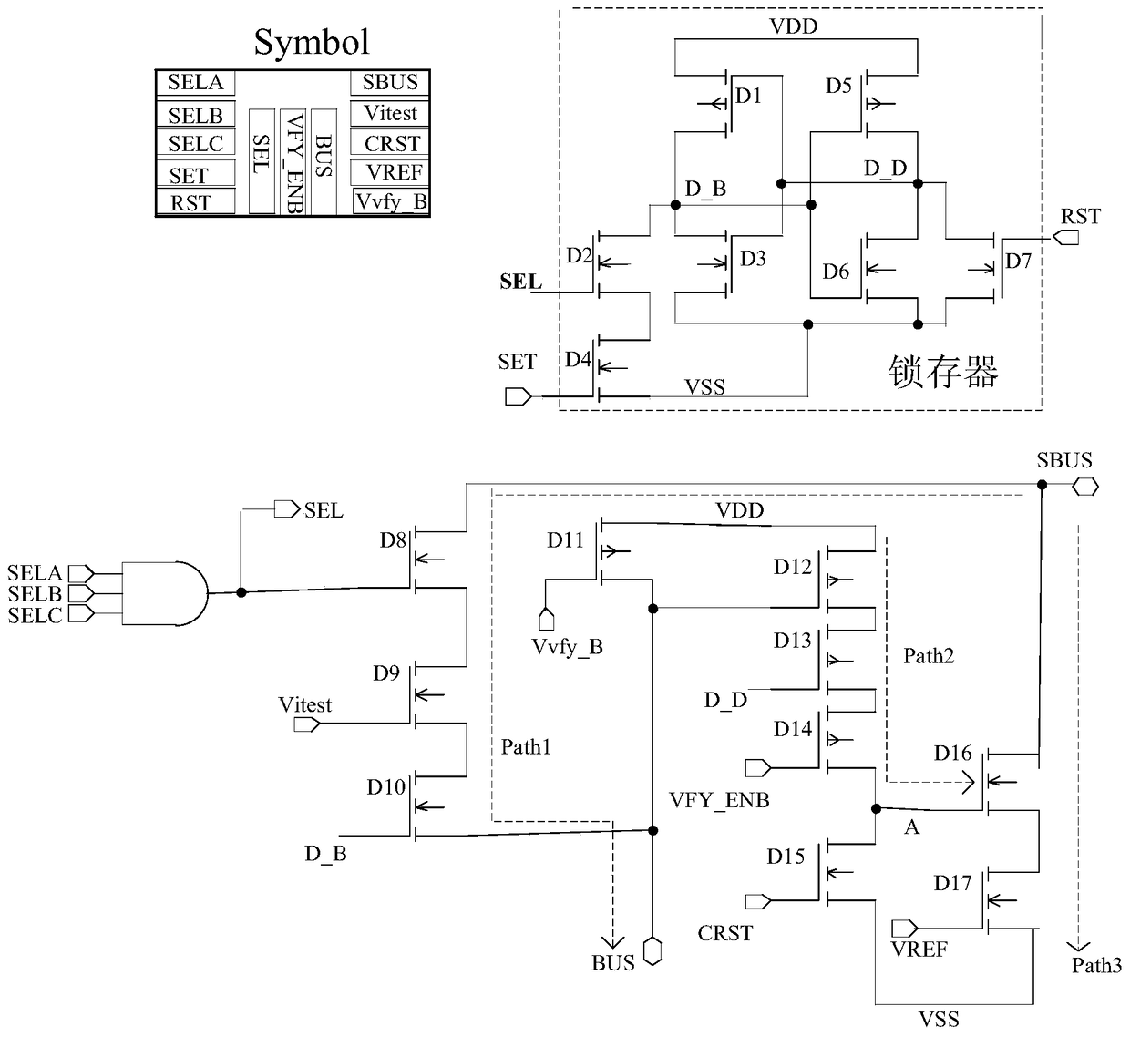
[0042] The chip includes storage units, the storage units form a storage column, and the storage columns form a storage array. Therefore, the chip can be used as a memory to store data.

[0043] In order to ensure the reliability of the programming and erasing operations, after the programming or erasing operations of the chip are completed, verification is required to determine whether the programming or erasing operations are successful. Specifically, after writing data into the memory, it is necessary to check whether the memory stores the data, that is, to confirm whether the programming is successful. If the memory successfully stores the data, the programming is successful, otherwise the programming fails; similarly, after d...


PUM


Abstract

Embodiments of the invention provide a chip based test processing method and apparatus. The method comprises: when executing a test, controlling an output branch to be disconnected by using a latch so as to screen a current of an input port of a bad storage array, wherein the output branch is used for transmitting the current of the input port of the storage array to an output port; and detecting a current transmitted through a test branch in the output port, and determining a test result according to the detected current. According to the processing method and apparatus provided by the embodiments of the invention, bad arrays in chip storage arrays can be isolated, and current influences of the bad arrays can be eliminated, so that the current of the output port can be accurately detected, and the accuracy of the test result is ensured.

Description

technical field [0001] The invention relates to the technical field of chips, in particular to a chip-based test processing method and a chip-based test processing device. Background technique [0002] In daily work, in order to ensure the reliability of programming and erasing operations, after the programming or erasing operations of the chip are completed, it is necessary to perform a verification (Verify) to determine whether the programming or erasing operations are successful. [0003] Currently, Verify is verified by current. Taking the detection of whether the programming of the flash memory (NAND FLASH) is successful as an example, by detecting the magnitude of the current at the NAND FLASH output port (such as the SBUS port), and comparing it with the preset reference current, it is determined whether the programming is successful. [0004] However, there are usually bad storage columns in the storage array of NAND FLASH. When designing NAND FLASH, some replacemen...

Claims


Application Information

Patent Timeline
Patent Type & Authority Patents(China)
IPC IPC(8): G11C29/56
Inventor 苏志强丁冲陈立刚谢瑞杰
Owner GIGADEVICE SEMICON (BEIJING) INC
Learn More