
Method for producing copper-free area between layers of printed board

A production method and copper-free area technology, applied in printed circuit manufacturing, printed circuit, multi-layer circuit manufacturing, etc., can solve the problems of process capacity reduction, unit cost increase, impedance, board thickness and other quality that cannot meet customer requirements, etc. Achieve the effect of reducing costs and increasing production capacity

Inactive Publication Date: 2017-05-10
SHENZHEN SUNTAK MULTILAYER PCB
View PDF5 Cites 9 Cited by
  • Summary
  • Abstract
  • Description
  • Claims
  • Application Information

AI Technical Summary

Problems solved by technology

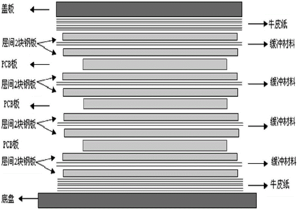
[0009] 1. Every time a board is pressed, it is necessary to use cushioning material to assist the pressing board, which increases the unit cost by 20% and reduces the production capacity of the process by 50%;
[0010] 2. The buffer material is a disposable material, which is not environmentally friendly;
[0011] The above-mentioned second method has the following defects: increasing the interlayer resin content will affect the thickness of the medium, which will cause the quality of impedance and board thickness to fail to meet customer requirements

Method used


Image

  • Method for producing copper-free area between layers of printed board
  • Method for producing copper-free area between layers of printed board
  • Method for producing copper-free area between layers of printed board

Examples


Embodiment Construction

[0033] In order to more fully understand the technical content of the present invention, the technical solutions of the present invention are further introduced and described below with reference to specific embodiments, but are not limited thereto.

[0034] like Figure 2 to Figure 4 The specific embodiment shown, this embodiment provides a method for manufacturing a copper-free area between layers of a printed circuit board, which can be used in the manufacturing process of a printed circuit board to realize the design of opening the interlayer resin PP to fill Hollow hollow. Specifically, it can be used in the pressing process of various multi-layer boards, especially for the production of small batches of circuit boards and prototype circuit boards.

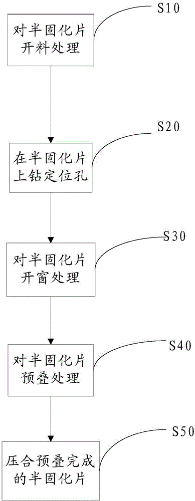
[0035] A method for manufacturing a copper-free area between layers of a printed board, comprising the following steps:

[0036] S10, open the prepreg;

[0037] S20, drilling positioning holes on the prepreg;

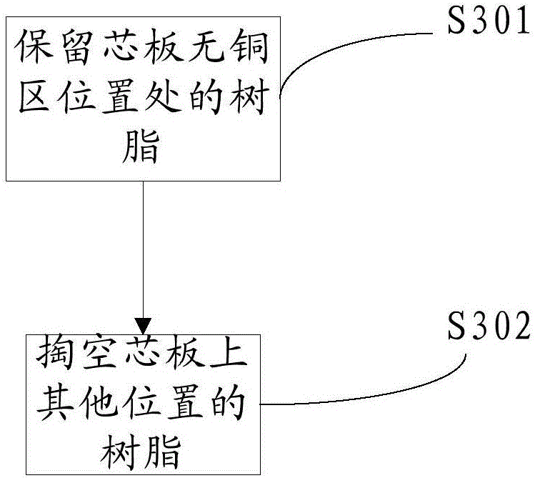
[0038] S30...


PUM


Abstract

The invention relates to a method for producing a copper-free area between layers of a printed board, comprising subjecting a prepreg to a blanking treatment; drilling a positioning hole in the prepreg; subjecting the prepreg to windowing treatment; subjecting the prepreg to pre-stacking treatment; and press fitting the pre-stacked prepreg. The method, by opening a window at a position close to a core board and then performing thepre-stacking and the lamination operations, guarantees that the laminated PCB has no empty edge, fills the recess position of the copper-free area, fills the cavity at a low level, reduces the cost, improves the production capacity, and does not affect the dielectric thickness.

Description

technical field [0001] The invention relates to a printed circuit board, and more particularly to a method for manufacturing a copper-free area between layers of a printed circuit board. Background technique [0002] Printed circuit boards (PCBs) appear in almost every electronic device. If there are electronic parts in a device, they are all mounted on PCBs of various sizes. In addition to fixing various small parts, the main function of the PCB is to provide the mutual electrical connection of the various parts above. As electronic devices become more and more complex, more and more parts are required, and the lines and parts on the PCB are also more and more dense. [0003] During the production process of the printed circuit board, when the circuit pattern is empty without copper area, the copper-free area here is in a low-lying position, which cannot be stressed during the lamination process, and there are tiny voids after the finished product. [0004] At present, w...

Claims


Application Information

Patent Timeline
IPC IPC(8): H05K3/46
CPCH05K3/4694H05K2203/068
Inventor 樊锡超姜雪飞邓辉
Owner SHENZHEN SUNTAK MULTILAYER PCB
Learn More