Pixel charge method and pixel charge circuit

一种像素充电、电路的技术,应用在非线性光学、静态指示器、仪器等方向,能够解决影响像素充电效果、减弱预充电实际效果、TFT导通不充分等问题,达到增强充电效果的效果

Active Publication Date: 2017-05-17
HKC CORP LTD +1
View PDF3 Cites 27 Cited by
  • Summary
  • Abstract
  • Description
  • Claims
  • Application Information

AI Technical Summary

Problems solved by technology

However, in order to reduce the capacitive coupling effect generated when the TFT (Thin Film Transistor, thin film transistor) switch is turned off, the gate drive voltage VGH of the TFT will be chamfered. However, when the pixel is precharged, the scan line The voltage waveform will reduce the scanning potential due to the chamfering process, which will make the TFT conduction insufficient during charging, thus affecting the charging effect of the pixel, and weakening the actual effect of pre-charging to a certain extent

Method used


Image

  • Pixel charge method and pixel charge circuit
  • Pixel charge method and pixel charge circuit
  • Pixel charge method and pixel charge circuit

Examples


Embodiment Construction

[0021] The following will clearly and completely describe the technical solutions in the embodiments of the present invention with reference to the drawings in the embodiments of the present invention. Apparently, the described embodiments are some, but not all, embodiments of the present invention. Based on the embodiments of the present invention, all other embodiments obtained by persons of ordinary skill in the art without making creative efforts belong to the protection scope of the present invention.

[0022] It should be understood that when used in this specification and the appended claims, the terms "comprising" and "comprises" indicate the presence of described features, integers, steps, operations, elements and / or components, but do not exclude one or Presence or addition of multiple other features, integers, steps, operations, elements, components and / or collections thereof.

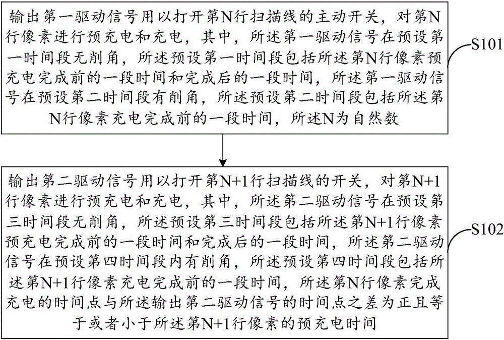
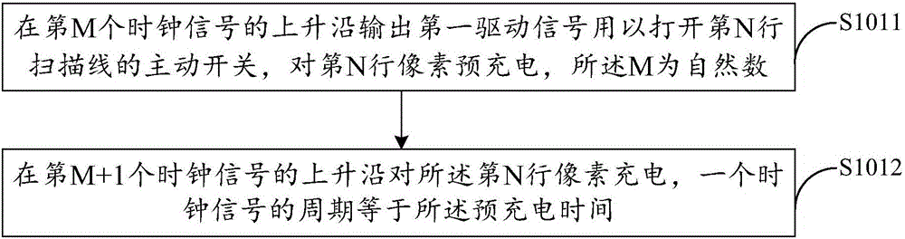
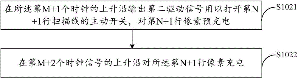
[0023] Please refer to figure 1 , figure 1 A pixel charging method provided in an emb...


PUM


Abstract

The invention provides a pixel charge method and a pixel charge circuit. The method comprises the following steps: a first driving signal is output to turn on an active switch of an N scan line so that N pixels are precharged and charged; a second driving signal is output to turn on a switch of an (N+1) scan line so that (N+1) pixels are precharged and charged; and the first driving signal and the second driving signal have no chamfers during a period before the corresponding pixels are precharged and during a period after the corresponding pixels are precharged, the first driving signal and the second driving signal have chamfers during a period before the corresponding pixels are charged, and the second driving signal is output before the N pixels are charged. The two driving signals drive the adjacent two rows of the scan lines to charge the pixels, the other row of the scan lines is precharged when one row of the scan lines is charged, and no chamfers exit during a certain period before and after precharge is finished. Therefore, active switches are fully turned on when precharge of the pixels ends and the pixels start to be actually charged, the actual charge process is not affected, and charge effects of the pixels are improved.

Description

technical field [0001] The technical field of liquid crystal display of the present invention, in particular relates to a pixel charging method and circuit. Background technique [0002] At present, some high frame rate LCD TVs (above 120HZ) and TVs with Tri-gate (three-gate drive circuit) structure, due to the high gate scanning frequency, shorten the TFT turn-on time and easily cause insufficient charging. A common practice is to use pre-charge, that is, charge the voltage of the Nth row to the N+1th row in advance, and finally charge the correct voltage to the N+1th row. However, in order to reduce the capacitive coupling effect generated when the TFT (Thin Film Transistor, Thin Film Transistor) switch is turned off, the gate drive voltage VGH of the TFT will be chamfered. The voltage waveform will reduce the scanning potential due to the chamfering process, so that the TFT conduction is insufficient during charging, thereby affecting the charging effect of the pixel, an...

Claims


Application Information

Patent Timeline
Patent Type & Authority Applications(China)
IPC IPC(8): G09G3/36
CPCG09G3/3677G09G3/3696G09G3/3648G09G3/3611G09G3/3688G09G2310/0251G09G2310/08G02F1/136286G02F1/1368
Inventor 王明良
Owner HKC CORP LTD
Why Eureka
Try Eureka