OLED (organic light emitting display) packaging method and OLED packaging structure

一种封装方法、封装结构的技术,应用在有机发光器件结构、电气元件、电路等方向,能够解决破坏封装效果、不可控因素、工艺复杂等问题,达到提高封装效果、减少使用数量、生产成本低的效果

Active Publication Date: 2017-05-17
TCL CHINA STAR OPTOELECTRONICS TECH CO LTD
View PDF4 Cites 20 Cited by
  • Summary
  • Abstract
  • Description
  • Claims
  • Application Information

AI Technical Summary

Problems solved by technology

[0008] Commonly used thin film packaging structures such as figure 1 As shown, it includes multilayer inorganic layers 200 and multilayer organic layers 300 arranged alternately on the OLED device 100, and the areas of the multilayer inorganic layers 200 and multilayer organic layers 300 are equal. The advantage of this thin film encapsulation structure is that the preparation process Simple, only a single set of mask (Mask) is needed to complete the deposition of multi-layer inorganic layer 200, but the deposited inorganic layer 200 does not completely cover the organic layer 300, and the end of the organic layer 300 can be in contact with the air, providing a channel for water vapor to enter , thereby destroying the encapsulation effect
Therefore, another thin film packaging structure (such as figure 2 shown), which includes multiple layers of inorganic layers 200' and multiple layers of organic layers 300' alternately arranged on the OLED device 100'. The thin film encapsulation structure requires that the area of ​​the inorganic layer 200' above each organic layer 300' be equal. greater than the area of ​​the organic layer 300', so that each layer of organic layer 300' can be completely covered by the inorganic layer 200' above it, preventing water vapor from entering the device from the organic layer 300'. In the upward direction, the area of ​​the multi-layer inorganic layer 200' increases gradually, so multiple sets of masks are required to complete the deposition of the multi-layer inorganic layer 200'. During the preparation process, the mask board needs to be replaced many times, and the process is complicated. Easy to introduce uncontrollable factors

Method used


Image

  • OLED (organic light emitting display) packaging method and OLED packaging structure
  • OLED (organic light emitting display) packaging method and OLED packaging structure
  • OLED (organic light emitting display) packaging method and OLED packaging structure

Examples


preparation example Construction

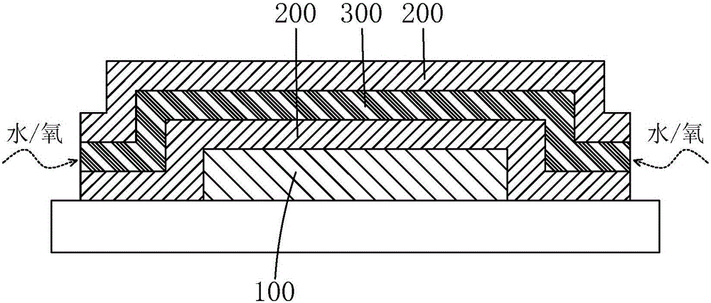
[0067] During the preparation process of the first organic layer 51, the first sealant 31 acts as a cofferdam to prevent overflow, and limits the size of the first organic layer 51, ensuring that the subsequent second inorganic layer 42 can be completely Covering the first organic layer 51 improves encapsulation effect.

[0068] Specifically, the thickness of the first organic layer 51 is 500 nm˜5 μm.

[0069] Specifically, the preparation method of the first organic layer 51 includes at least one of screen printing, spin coating, inkjet printing, and film casting.

[0070] Specifically, the first organic layer 51 is composed of organic resin. Preferably, the composition of the first organic layer 51 includes at least one of silicone resin and polymethyl methacrylate.

[0071] Specifically, the curing method of the first organic layer 51 includes at least one of thermal curing and UV curing. Preferably, the curing method of the first organic layer 51 is thermal curing.

[0...

example 1

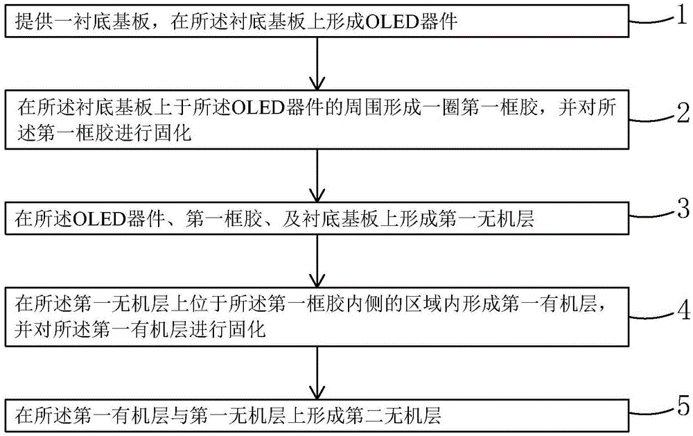
[0097] Step 1, such as Figure 4 As shown, a base substrate 10 is provided on which an OLED device 20 is formed.

[0098] Step 2, such as Figure 5 As shown, a circle of first sealant 31 is formed on the base substrate 10 around the OLED device 20 , and the first sealant 31 is cured.

[0099] The height of the first sealant 31 is 3 μm to 6 μm; the width of the first sealant 31 is 0.1 mm to 3 mm;

[0100] The distance between the inner edge of the first sealant 31 and the edge of the OLED device 20 is 1.0mm-1.5mm;

[0101] The main component of the first frame glue 31 is acrylic resin;

[0102] The curing method of the first sealant 31 is UV curing. During the UV curing process, the energy density of UV light is 3000mJ / cm 2 ~5000mJ / cm 2 , UV irradiation time is 30s ~ 100s.

[0103] Step 3, if Image 6 As shown, a first inorganic layer 41 is formed on the base substrate 10 and the OLED device 20, the first inorganic layer 41 covers the OLED device 20 and the first sealant...

example 2

[0112] Step 1, such as Figure 4 As shown, a base substrate 10 is provided on which an OLED device 20 is formed.

[0113] Step 2, such as Figure 5 As shown, a circle of first sealant 31 is formed on the base substrate 10 around the OLED device 20 , and the first sealant 31 is cured.

[0114] The height of the first rubber frame 31 is 10 μm to 15 μm; the width of the first rubber frame 31 is 1 mm to 2 mm;

[0115] The distance between the inner edge of the first sealant 31 and the edge of the OLED device 20 is 1.5mm-2mm;

[0116] The main component of the first sealant 31 is silicone resin;

[0117] The curing method of the first sealant 31 is thermal curing, and the thermal curing conditions are as follows: a heating temperature of 60° C. to 90° C. and a heating time of 30 minutes to 100 minutes.

[0118] Step 3, if Image 6 As shown, a first inorganic layer 41 is formed on the base substrate 10 and the OLED device 20, the first inorganic layer 41 covers the OLED device ...


PUM


Abstract

The invention provides an OLED (organic light emitting display) packaging method and an OLED packaging structure. The OLED packaging method is combined with the frame glue packaging technology and the thin film packaging technology, organic layers coffered with frame glue can be limited in size, each organic layer is assuredly covered by an organic layer above the same completely, and packaging effect is improved; meanwhile, the organic layers can be prepared with one mask set, use amount of the masks is reduced, and production cost is saved. The OLED packaging structure is combined with the frame flue packaging structure and the thin film packaging structure, the organic layers coffered with the frame glue can be limited in size, the organic layers are assuredly covered with the organic layer above the same completely, good packaging effect is achieved, meanwhile, the organic layers can be prepared with one mask set, and production cost is low.

Description

technical field [0001] The invention relates to the field of display technology, in particular to an OLED packaging method and an OLED packaging structure. Background technique [0002] Organic Light Emitting Display (OLED) has self-illumination, low driving voltage, high luminous efficiency, short response time, high definition and contrast, nearly 180° viewing angle, wide operating temperature range, and can realize flexible display and With many advantages such as large-area full-color display, it is recognized by the industry as a display device with the most potential for development. [0003] According to the driving method, OLED can be divided into two categories: passive matrix OLED (Passive Matrix OLED, PMOLED) and active matrix OLED (Active Matrix OLED, AMOLED), namely direct addressing and thin film transistor matrix addressing. Among them, AMOLED has pixels arranged in an array, belongs to the active display type, has high luminous efficiency, and is usually use...

Claims


Application Information

Patent Timeline
Patent Type & Authority Applications(China)
IPC IPC(8): H01L51/52H01L51/56
CPCH10K50/8426H10K2102/302H10K71/00H10K50/8445
Inventor 李文杰
Owner TCL CHINA STAR OPTOELECTRONICS TECH CO LTD
Why Eureka
Try Eureka