Terminal equipment, reading and writing equipment, data transmission system and hardware initializing method
- Summary
- Abstract
- Description
- Claims
- Application Information
AI Technical Summary
Problems solved by technology
Method used
Image

Examples
Embodiment 1
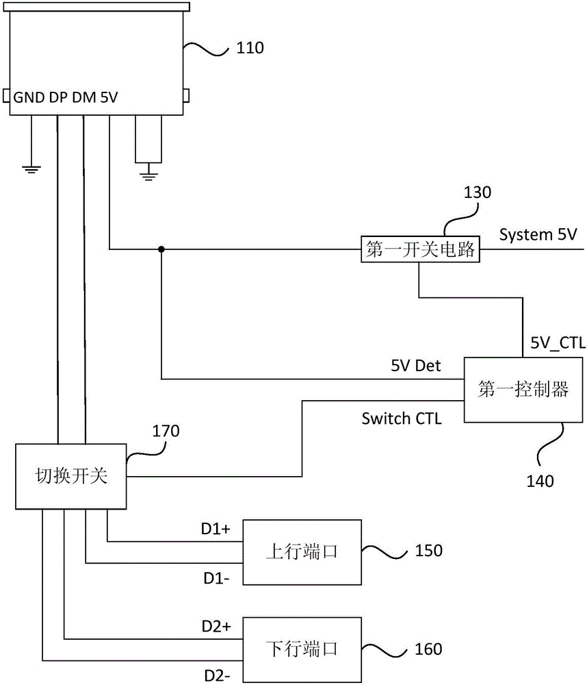
[0042] Figure 1a It is a structural diagram of a terminal device provided in Embodiment 1 of the present invention. The structure of the terminal device in this embodiment specifically includes:
[0043] A first universal serial bus interface 110, an uplink port 150, a downlink port 160, a switch 170, a first controller 140 and a first switch circuit 130;
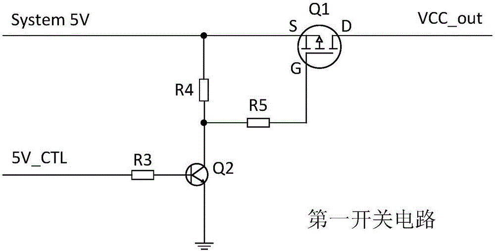
[0044] The first universal serial bus interface 110 is used to connect with the universal serial bus interface of external equipment, and its signal pin is grounded; the upstream port 150 and the downstream port 160 are all connected to the first universal serial bus interface 110 by a switch 170 The data transmission end of the first switch circuit 130 is connected to the power supply pin of the first universal serial bus interface 110, and the second end of the first switch circuit 130 is connected to the on-off state through the switch 170. Input power, generally 5V system power, that is, System 5V;
[0045] The first ...
Embodiment 2
[0054] Embodiment 2 of the present invention provides a structural diagram of a terminal device. This embodiment is optimized on the basis of the above embodiments. In this embodiment, if figure 2 As shown, it also includes: a current limiting circuit 120, the first end of the current limiting circuit 120 is connected to the power supply pin of the first universal serial bus interface 110 (that is, the pin for outputting or accessing +5V), and the current limiting circuit 120 The third end of the first controller 140 is connected to the signal input end for outputting a signal 5V Det, and the second end of the current limiting circuit 120 is connected to the first end of the first switch circuit 130;
[0055] Further, the current limiting circuit 120 is optimized to: include a current limiting switch 180, a resistor R1 and a resistor R2; The pin is connected, and is used for outputting the supply voltage USB5V to the power supply pin of the first universal serial bus interfa...
Embodiment 3
[0062] Figure 3a A structural diagram of a read-write device provided in Embodiment 3 of the present invention, specifically including:
[0063] The second universal serial bus interface 230, the second controller 250, the trigger circuit 240, the second switch circuit 210 and the third switch circuit 220; the signal pin Signal_GND of the second universal serial bus interface 230 is connected to the trigger The detection terminal of the circuit 240 is connected, and the feedback terminal of the trigger circuit 240 is connected with the signal input terminal of the second controller 250. In this embodiment, the signal transmitted between the two is defined as Insert Det, which is specifically used for Describe the voltage state of the second universal serial bus interface 230 access;
[0064] The signal pin of the second universal serial bus interface 230 is used to be connected with the signal pin of the first universal serial bus interface 110; The data processing end of th...
PUM
 Abstract
Description
Claims
Application Information
PatSnap Eureka turns technology decisions into work you can execute. Powered by our Innovation Knowledge Graph, it runs expert workflows across engineering, life sciences, materials and intellectual property. Get your review-ready output in minutes.


