Semiconductor component overturning device and test equipment thereof

A test equipment, semiconductor technology, applied in semiconductor/solid-state device manufacturing, electrical components, conveyor objects, etc., can solve the problem that semiconductor components cannot be picked and placed at the same time

Inactive Publication Date: 2017-05-31
KING YUAN ELECTRONICS
View PDF3 Cites 1 Cited by
  • Summary
  • Abstract
  • Description
  • Claims
  • Application Information

AI Technical Summary

Problems solved by technology

[0003] However, after the above-mentioned inversion is completed, the inversion device needs to be inverted 180 degrees to return to the original position before it can carry the next batch

Method used


Image

  • Semiconductor component overturning device and test equipment thereof
  • Semiconductor component overturning device and test equipment thereof
  • Semiconductor component overturning device and test equipment thereof

Examples


Embodiment Construction

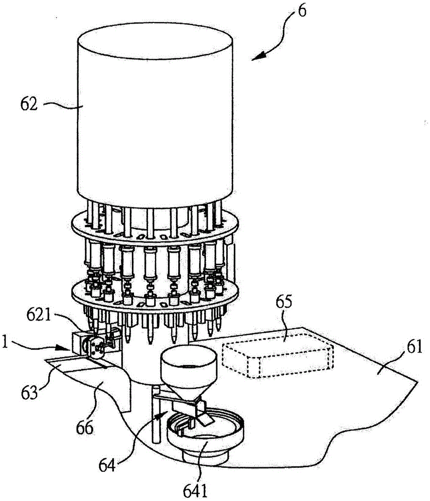
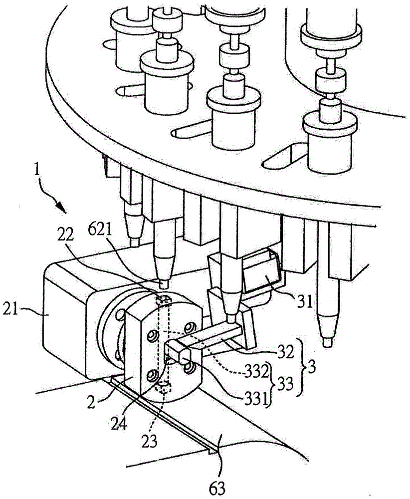
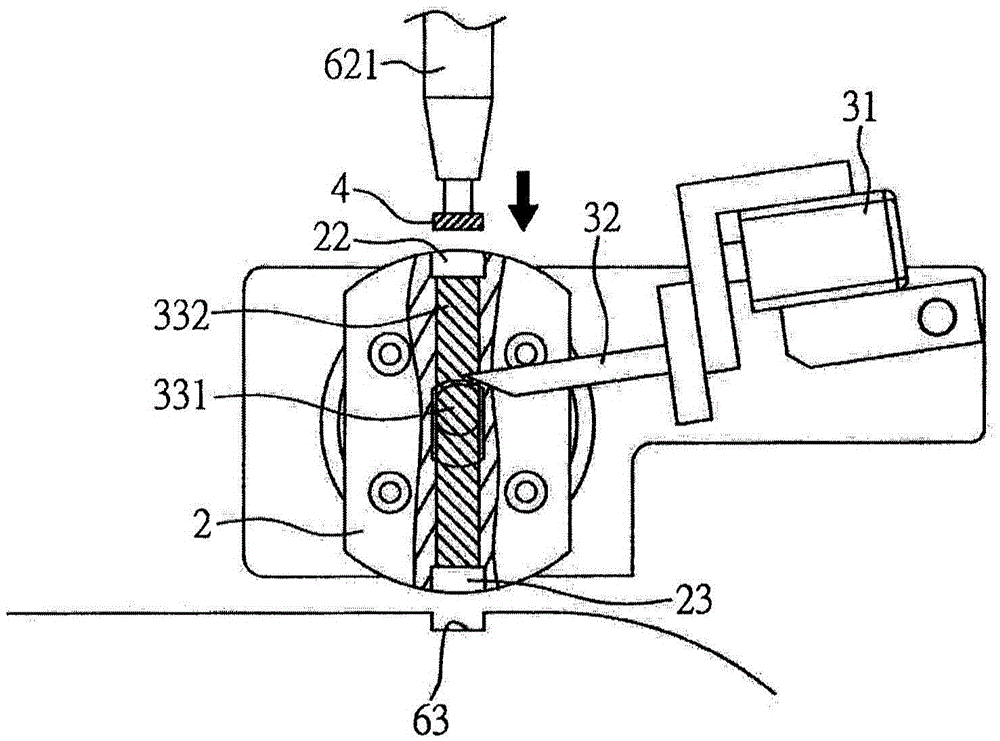
[0023] see figure 1 and figure 2 , is a perspective view of the semiconductor element inversion testing equipment and a perspective view of the semiconductor element inversion device according to the first embodiment of the present invention. Such as figure 1 As shown, first viewed from the whole, the semiconductor device inversion testing equipment of the present invention includes a semiconductor device inversion device 1 and a sorting machine 6 . In this embodiment, the sorting machine 6 includes a turret 62 arranged on a working table 61 and a feeding area 64, a testing area 65 and a discharging area 66 arranged around the turret 62, wherein The material area 64 can be a vibrating plate (Bowl feeder) 641 , and the output area 66 includes a packaging roll 63 . The turret 62 includes a plurality of suction heads 621 arranged at intervals at an angle, one end of which sucks a semiconductor element 4 from the feed area 64 and rotates to the test area 65, and then turns t...


PUM


Abstract

The invention relates to a semiconductor component overturning device and test equipment thereof. The semiconductor component overturning device comprises a turntable, a linkage unit and a controller; the turntable sleeves a motor; at least two containing grooves separately connected with a vacuum tube are arranged at the end edge of the turntable; furthermore, a containing space is in the turntable; the linkage unit comprises a driving part and a driven part; the driving part is connected to a driving device; the driven part is contained in the containing space, wherein the driving part and the driven part have a linkage relationship; and the controller is separately connected to the motor and the driving device electrically, and used for sequentially controlling the action moments of the turntable and the linkage unit. Thereby, multiple semiconductor components can be continuously overturned by utilization of a mechanism module, which is simple and low in cost; the capacity per unit time can be greatly improved; and thus, the overturning efficiency can be effectively increased.

Description

technical field [0001] The invention relates to a semiconductor element inversion device and its testing equipment, especially to a semiconductor element inversion device and its testing equipment suitable for front and back conversion. Background technique [0002] Known technologies such as the semiconductor element flipping device and method disclosed in Taiwan Patent Publication No. I462240, please refer to Figure 13 , is a continuous operation diagram of a known semiconductor element flipping device. As shown in the figure, the openable first platform 930 and the second platform 932 are connected by a turning shaft 928. The turning shaft 928 includes a first shaft and a second shaft which are coaxial and can rotate separately or simultaneously. The first carrier 934 has a plurality of trays 924 carrying semiconductor components, and the second carrier 938 has the same number of trays 924 not carrying semiconductor components. After the first platform 930 and the secon...

Claims


Application Information

Patent Timeline
IPC IPC(8): H01L21/67H01L21/677
CPCH01L21/67242H01L21/677
Inventor 詹勋亮罗伟诚陈俞成蔡旻谚
Owner KING YUAN ELECTRONICS
Why Eureka
Try Eureka