

Semiconductor processing device and method
A processing device and processing method technology, applied in semiconductor/solid-state device manufacturing, electrical components, circuits, etc., can solve the problems of difficult detection, large processing fluid, difficult to be accurately controlled, etc., and achieve the effect of saving consumption
- Summary
- Abstract
- Description
- Claims
- Application Information
AI Technical Summary
Problems solved by technology
Method used
Image

Examples
Embodiment Construction
[0052] In order to make the above objects, features and advantages of the present invention more comprehensible, the present invention will be further described in detail below in conjunction with the accompanying drawings and specific embodiments.
[0053]The term "one embodiment" or "embodiment" here refers to that specific features, structures or characteristics related to the embodiment can be included in at least one implementation of the present invention. The appearances of "in one embodiment" in various places in this specification do not necessarily all refer to the same embodiment, nor do they necessarily refer to a separate or selected embodiment that is mutually exclusive of other embodiments. "Multiple" and "several" in the present invention mean two or more. "And / or" in the present invention means "and" or "or".
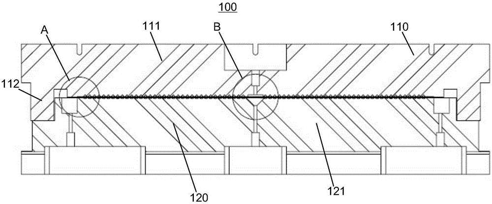
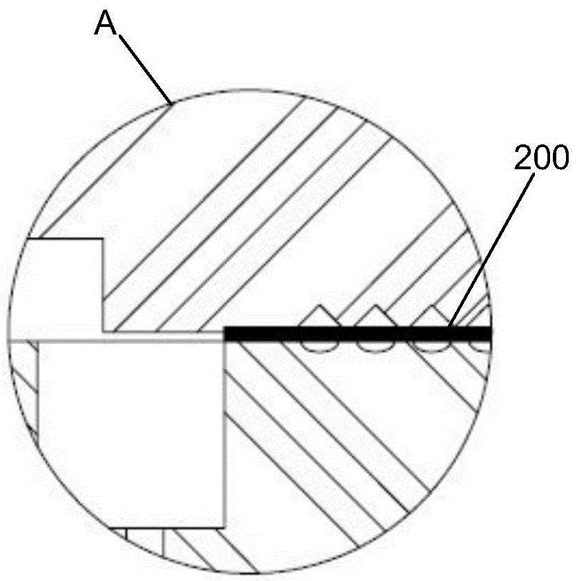
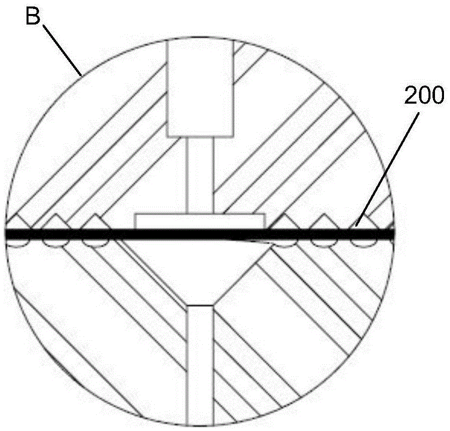
[0054] The invention provides a semiconductor processing device, which can precisely control the flow direction and flow speed of the processing fluid...
PUM
 Abstract
Description
Claims
Application Information