Ring cavity nano-wire electric injection single-photon source device

A single photon source, nanowire technology, applied in electrical components, semiconductor devices, circuits, etc., can solve the problems of difficult preparation, small structure size in the short-wave band, and poor compatibility between photonic crystal microcavities and electrical injection devices. , to achieve the effect of enhancing radiation efficiency, improving directionality, and improving light collection and utilization efficiency

Inactive Publication Date: 2017-05-31
INST OF ELECTRONICS ENG CHINA ACAD OF ENG PHYSICS
View PDF6 Cites 7 Cited by
  • Summary
  • Abstract
  • Description
  • Claims
  • Application Information

AI Technical Summary

Benefits of technology

The present technology allows for efficient emission of particles called quantum dots (QDS) by injecting them into an optoacoustic waveguide or other type of structure through electric fields. This helps create high brightness sources without being affected by external factors like temperature changes or vibrations. Additionally, this technology has potential applications such as generating individualized images on demand at different wavelengths levels within specific spectral ranges.

Problems solved by technology

This patents discusses different ways how to enhance the performance (efficiency) of generating singly charged particles called quantum dods during certain types of experiments like laser scanning fluorescein analysis. These techniques involve placing quantum dodes into specific areas within a microscope chamber where they actively produce signals while minimizing unwanted side effects caused by ambient radiation. Additionally, these methods aim at enhancing the ability to generate highly pure mono phosphorus diode lights (MPDLs), which have applications beyond electronic security systems.

Method used


Image

  • Ring cavity nano-wire electric injection single-photon source device
  • Ring cavity nano-wire electric injection single-photon source device
  • Ring cavity nano-wire electric injection single-photon source device

Examples


Embodiment 1

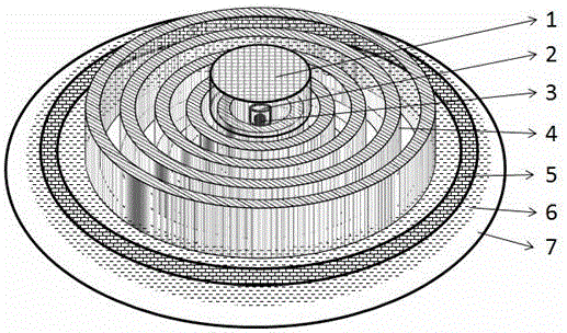
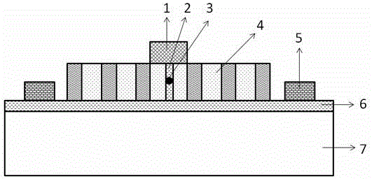
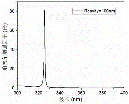
[0028] An AlGaN / GaN ring cavity nanowire electrical injection single photon source based on graphene transparent p-type electrodes. Such as figure 1 , 2 As shown, among them: 1 is graphene transparent p-type electrode; 2 is p-AlGaN / i-AlGaN / GaN-Qdot / i-AlGaN / n-AlGaN nanowire; 3 is GaN embedded in pin AlGaN nanowire Quantum dots; 4 is a multilayer concentric ring cavity composed of AlGaN and spin-on-coated glass (SOG), and the thickness of the concentric ring cavity is a quarter of the equivalent wavelength; 5 is an n-type electrode composed of Pt / Au; 6 is n-type AlGaN epitaxial material; 7 is an AlN substrate. This structure consists of a Bragg grating composed of multi-layer concentric ring cavities to limit the photons diverging in the two spatial dimensions of the vertical nanowire, and only emit single photons along the two ends of the nanowire, which has good directionality, and the concentric ring microcavity The increase of photon density in the localized state greatly...

Embodiment 2

[0032] An InGaAs / InAs ring cavity nanowire electrical injection single photon source based on Ti / Au highly reflective p-type electrodes. Such as figure 1 , 2 As shown, among them: 1 is Ti / Au highly reflective p-type electrode; 2 is p-InGaAs / i-InGaAs / InAs / i-InGaAs / n-InGaAs nanowire; 3 is InAs embedded in pin InGaAs nanowire Quantum dots; 4 is Al 2 o 3 The thickness of the concentric ring cavity is a quarter of the equivalent wavelength; 5 is an n-type electrode composed of Ni / Au; 6 is an n-type InGaAs epitaxial material; 7 is a GaAs substrate. This structure consists of a Bragg grating composed of multilayer concentric ring cavities to confine photons diverging in the two spatial dimensions of the vertical nanowire, and a Ti / Au highly reflective p-type electrode confines photons diverging along the p-type end of the nanowire, so that only along the nanowire The supersubstrate at one end of the line n-type emits single photons downwards, and the increase of local state photo...


PUM


Abstract

The invention discloses a ring cavity nano-wire electric injection single-photon source device. The ring cavity nano-wire electric injection single-photon source device is characterized by comprising a p type electrode, a pin nano-wire, a quantum dot embedded into the nano-wire, a multilayer concentric ring cavity, an n type electrode, an n type material and a substrate. The device has the advantages that while electric injection work is achieved, an annular Bragg micro-cavity composed of multilayer concentric rings is utilized, an electromagnetic field is generated at the concentric quantum dot position, and the local area is enhanced; the radiation efficiency of a quantum dot single-photon source can be enhanced through a Purcell effect, divergence of photons can be limited in two spatial dimensions vertical to the nano-wire, the single photons can be emitted only in the nano-wire direction, the single photons are easily coupled with optical fibers, and the light collecting and utilizing efficiency is greatly improved. The ring cavity nano-wire electric injection single-photon-source device can be widely applied to quantum information, quantum computing, quantum authentication and quantum precision measurement relevant fields.

Description


Claims


Application Information

Patent Timeline
Owner INST OF ELECTRONICS ENG CHINA ACAD OF ENG PHYSICS
Why Eureka
Try Eureka