Photo-semiconductor device and method of manufacturing the same

a photo-semiconductor and semiconductor technology, applied in the field of photo-semiconductor, can solve the problems of not being able to use such an ideal structure, not being able to directly form a photoconductive film, and not being able to use glass substrates to form photoconductive films, etc., to achieve improved thz radiation efficiency, low cost, and improved thermal characteristics of elements

Inactive Publication Date: 2005-09-29
CANON KK
View PDF18 Cites 51 Cited by
  • Summary
  • Abstract
  • Description
  • Claims
  • Application Information

AI Technical Summary

Benefits of technology

[0017] With either of the above-described two methods, it is possible to integrally form a photoconductive element on an Si semispherical lens as thin film in order to suppress the substrate mode and improve the THz radiation efficiency. Additionally, the thermal characteristics of the element are improved when it is integrally formed on a highly thermally conductive substrate made of AlN or SiC. When film type photoconductive elements according to the invention are integrally formed on a substrate on which high frequency transmission lines such as microstrip lines are arranged, it is possible to provide a compact sensing module at low cost. Additionally, when film type photoconductive elements according to the invention are integrally formed on Si-IC gates that require a high speed switching feature, it is possible to provide an optically a

Problems solved by technology

However, it has not been possible to use such an ideal structure because it is not possible to form a photoconductive film that operates satisfactorily on an Si substrate.
However, a photoconduc

Method used


Image

  • Photo-semiconductor device and method of manufacturing the same
  • Photo-semiconductor device and method of manufacturing the same
  • Photo-semiconductor device and method of manufacturing the same

Examples


example 1

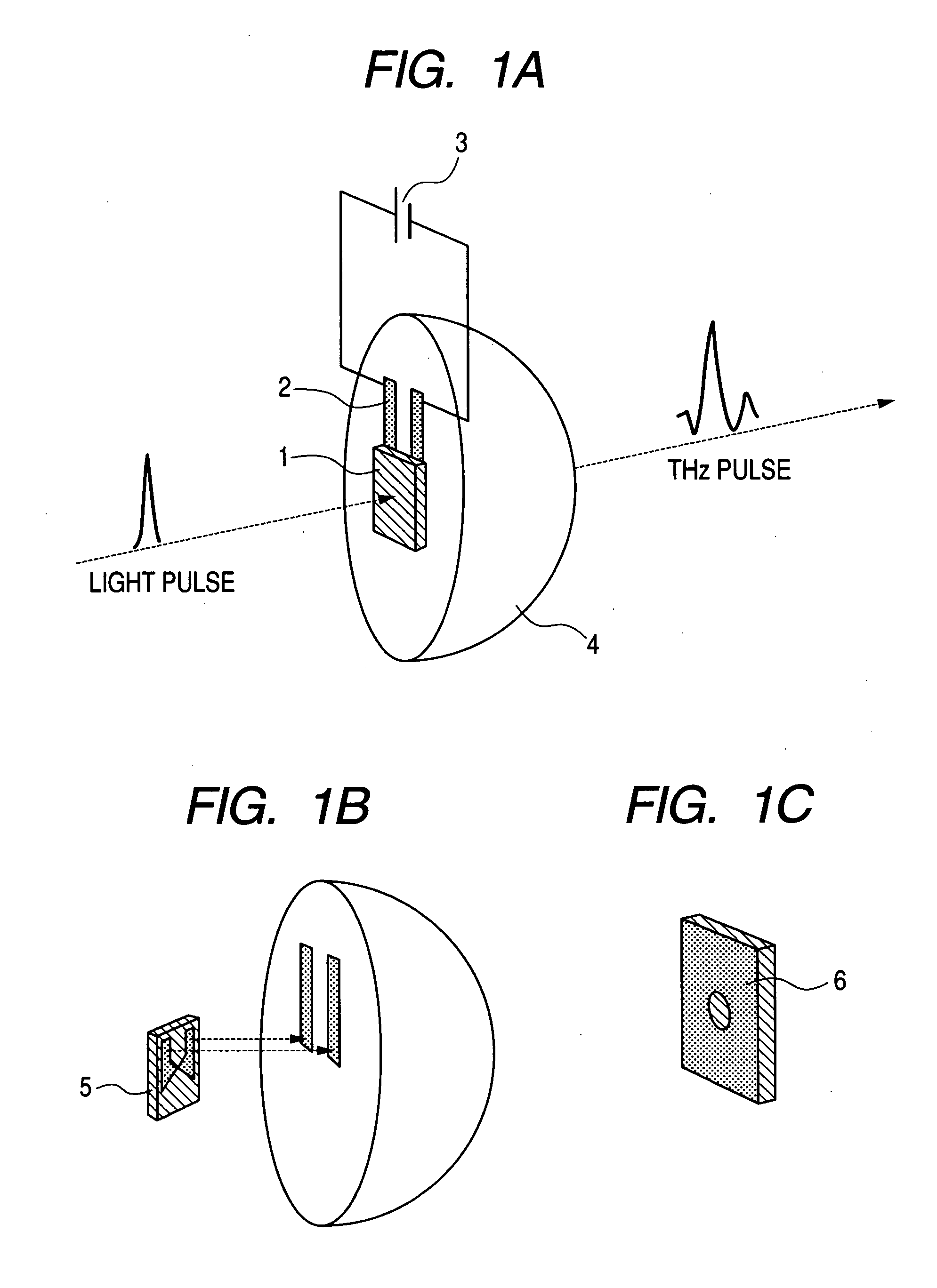
[0030] In this example, a photoconductive element is directly and integrally formed on an Si lens in order to improve the radiation efficiency from the photoconductive switch to space. FIG. 1A is a schematic perspective view of the ultimately integrally formed element. Two Ti / Au electrodes 2 are formed on the bottom surface of a semispherical lens 4 made of electrically highly resistive Si in order to supply a bias voltage. The photoconductive element 1 is integrally formed to show a configuration as illustrated in FIG. 1A where an antenna 5 is formed with a gap of 5 μm arranged to separate it into two parts on the surface of a GaAs layer grown at low temperature (LT-GaAs) as photoconductive film, as illustrated in FIG. 1B, and brought into electrode contact with bias voltage supply lines 2.

[0031] The photoconductive film shows a thickness of about 1.5 μm after removing the GaAs substrate that was used for epitaxial growth. When the photoconductive element 1 is transferred onto the...

example 2

[0045] In the second example, a film type photoconductive element like the one prepared in Example 1 is bonded to a thermally highly conductive substrate in order to prevent the characteristics of the element from being degraded by elevated temperatures.

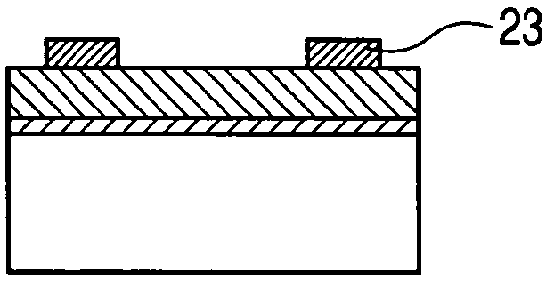
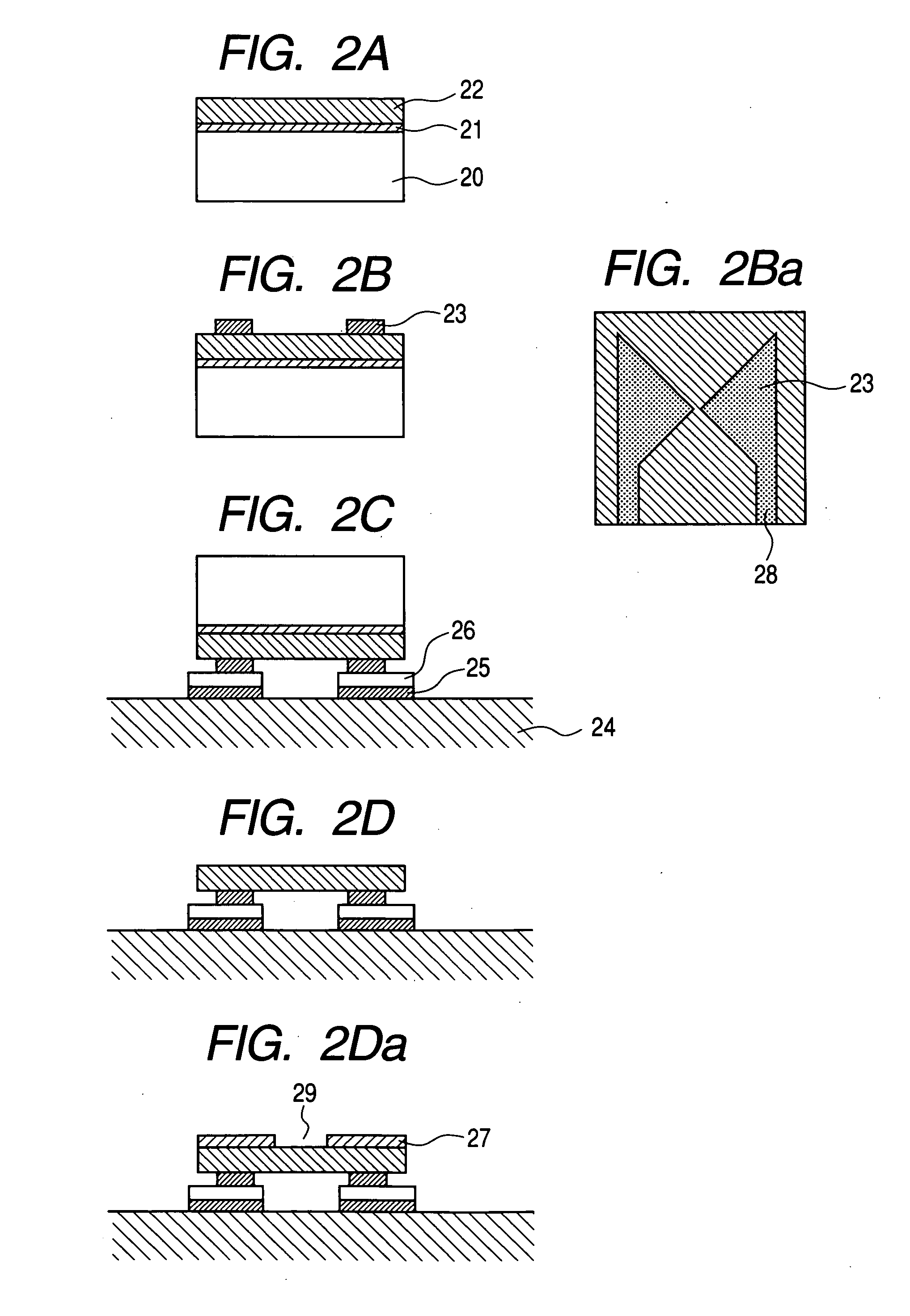
[0046]FIGS. 3A, 3B, 3C and 3D are schematic illustrations of an embodiment of integrated device according to the invention and prepared in Example 2, showing the device in different manufacturing steps. The components same as those of the embodiment of example 1 are denoted respectively by the same reference symbols and will not be described further. The process is the same as that of Example 1 down to the step of forming an antenna as shown in FIGS. 3A and 3B. Referring now to FIG. 3C, after cutting out a chip, the antenna is bonded by using a resin adhesive or the like 31 at the front surface thereof to a hold substrate 30 that is typically made of glass and then the GaAs substrate is removed by means of a technique similar to the...

example 3

[0049] In this example, photoconductive elements according to the invention are applied to an integrated type THz wave sensing module as shown in FIGS. 5A and 5B. The configuration for the module will be described below by referring to FIG. 5A. Optical waveguides 55, 56, 62 and an optical divider / coupler 57, 58 are three-dimensionally formed in a substrate 50, which is made of a transparent polymer material such as polyimide with a modified refractive index. The work may be prepared by molding some of the components and assembling them or by using a technique of forming three-dimensional waveguides by means of a laser. Materials that can be used include quartz, glass, plastics and polymers, some of which may not be transparent. It is advisable to use a material that is practically free from loss of light at least for the waveguides. It is desirable to apply a material (not shown) that shows excellent high frequency characteristics such as polyimide or BCB to the surface where coplan...


PUM


Abstract

A photo-semiconductor device comprises a photoconductive semiconductor film provided with electrodes and formed on a second substrate, the semiconductor film being formed by epitaxial growth on a first semiconductor substrate different from the second substrate, the second substrate being also provided with electrodes, the electrodes of the second substrate and the electrodes of the photoconductive semiconductor film being held in contact with each other.

Description

BACKGROUND OF THE INVENTION [0001] 1. Field of the Invention [0002] This invention relates to a photo-semiconductor device having a function of transmitting / receiving a high frequency electric signal mainly in a frequency range between milli-meter and tera-hertz waves and a method of manufacturing the same. [0003] 2. Related Background Art [0004] So-called non-destructive sensing technologies using electromagnetic waves of a frequency range between milli-meter and tera-hertz waves (30 GHz to 30 THz) have been developed in recent years. Technologies using electromagnetic waves of such a frequency range include those for imaging, using fluoroscopic inspection apparatus that are safe and can replace X-ray apparatus, those for examining the internally bonded states of substances by determining absorption spectra and complex dielectric constants, those for analyzing biomolecules and those for evaluating carrier densities and carrier mobilities. Position sensing technologies have also bee...

Claims


Application Information

Patent Timeline
IPC IPC(8): H01L21/00H01L21/44H01L21/48
CPCH01L31/022408H01L31/0232G01J3/42G01J3/0256G01N21/3581H01L31/101H01L2224/16225H01L2224/32225H01L2224/73204H01L31/02325H01Q9/285H01L2924/00H01L31/09H01L33/36
Inventor OUCHI, TOSHIHIKO
Owner CANON KK
Why Eureka
Try Eureka