Touch control display panel
A technology of touch display panel and display area, applied in the fields of instruments, electrical digital data processing, character and pattern recognition, etc. Adverse effects, reduce the frame area, improve the stability of the effect
Active Publication Date: 2017-06-06
XIAMEN TIANMA MICRO ELECTRONICS
8 Cites 26 Cited by
AI-Extracted Technical Summary
Problems solved by technology
However, when the fingerprint recognition is set in the non-display area, it is not conducive to the narrow frame design of the display device. When it is set on the back, the thickness of the display device increases, which is not conducive to the thinner design; and the ...
View moreAbstract
The application discloses a touch control display panel. The touch control display panel comprises a display area, and further comprises a colored film substrate, a cover plate and a fingerprint detection electrode, wherein the fingerprint detection electrode is arranged in the display area, the fingerprint detection electrode is located between the colored film substrate and the cover plate, and the fingerprint detection electrode is used for receiving fingerprint detection signals, and generates fingerprint sensing signals according to sensed fingerprints. The touch control display panel can achieve lighting and thinning and narrow bezel design of a display device having a fingerprint detection function.
Application Domain
Technology Topic
Image
Examples
- Experimental program(1)
Example Embodiment
[0036] The application will be further described in detail below with reference to the drawings and embodiments. It can be understood that the specific embodiments described here are only used to explain the related invention, but not to limit the invention. In addition, it should be noted that, for ease of description, only the parts related to the relevant invention are shown in the drawings.
[0037] It should be noted that the embodiments in the application and the features in the embodiments can be combined with each other if there is no conflict. Hereinafter, the present application will be described in detail with reference to the drawings and in conjunction with embodiments.
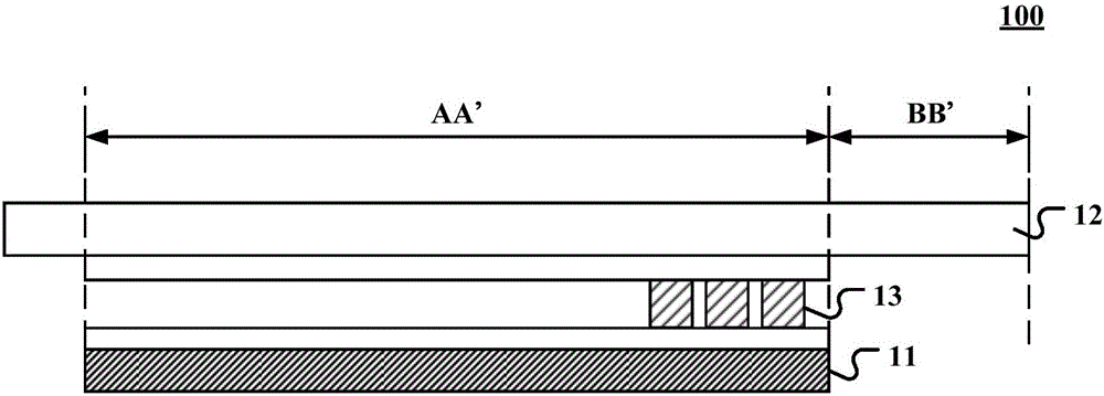
[0038] Please refer to figure 1 , Which shows a schematic diagram of a cross-sectional structure of the touch display panel according to the present application. The touch display panel 100 includes a display area AA' and a non-display area BB'. The display area AA' is an area on the touch display panel 100 that can display pictures and can sense touch, and the non-display area BB' contains electrical components and circuits for driving the display devices and touch devices in the display area to work. Area.
[0039] Such as figure 1 As shown, the touch display panel 100 includes a color filter substrate 11, a cover plate 12 and fingerprint detection electrodes 13. The fingerprint detection electrode 13 is arranged in the display area AA', and the fingerprint detection electrode 13 is located between the color filter substrate 11 and the cover plate 12. The fingerprint detection electrode 13 may be a metal electrode or an electrode formed of other conductive materials such as ITO (Indium Tin Oxide) for receiving fingerprint detection signals and generating fingerprint detection signals according to the fingerprints sensed.
[0040] In this embodiment, through the contact between the finger skin and the touch display panel, the depth and shape of the dimples at different positions in the fingerprint are identified to obtain the three-dimensional information of the fingerprint. Specifically, the fingerprint detection electrode can form a capacitance with other conductive materials (such as touch electrodes) in the touch display panel, and a capacitance can also be formed between different fingerprint detection electrodes, or a capacitance can also be formed between the fingerprint detection electrode and the ground. When a finger touches the display panel, the surface of the finger forms a capacitance with the fingerprint detection electrode, and because the degree of unevenness of the fingerprint at different positions is different, the capacitance formed by the fingerprint detection electrode is also different. When detecting a fingerprint, it can be considered that the capacitance formed by the surface of the finger and the fingerprint detection electrode is connected to the fingerprint detection electrode and other conductive materials in the touch display panel, or the fingerprint detection electrode and the ground, or the fingerprint. In a circuit that detects the capacitance between the electrodes, the signal strength in the circuit changes. At this time, the amount of capacitance change can be obtained by the amount of change in signal strength, and the size of the capacitance formed by the surface of the finger and the fingerprint detection electrode can be obtained, and then the distance between the surface of the finger and the fingerprint detection electrode can be obtained. The two-dimensional shape and depth information of the fingerprint is obtained between different positions on the surface and the fingerprint detection electrode.
[0041] Specifically, when detecting a fingerprint, a fingerprint detection signal may be provided to the fingerprint detection electrode, and the fingerprint detection signal may be an AC signal. In this way, the signal strength in the circuit including the capacitance formed by the surface of the finger and the fingerprint detection electrode will change , So that the amount of charge sensed by the fingerprint detection electrode changes, the shape and texture of the fingerprint can be determined according to the fingerprint sensing signal returned by the fingerprint detection electrode.
[0042] From figure 1 It can be seen that in this embodiment, the fingerprint detection electrode is arranged in the display area AA', and the fingerprint detection electrode with smaller length, width, and thickness can be made on the color filter substrate by film formation. The fingerprint detection electrode and the finger The capacitance formed on the surface is used to determine the fingerprint texture. There is no need to design a large fingerprint sensor, which reduces the volume of electrical components used to realize the fingerprint detection function, improves the integration of fingerprint detection devices, and facilitates the realization of touch display panels. Narrow frame and thin design. In addition, the fingerprint detection electrode can be arranged in the display area without opening in the housing of the display device, so that impurities such as water stains and dust can be prevented from entering the interior of the display device through the opening, and the stability of the display device can be improved.
[0043] In the touch display panel 100, the cover 12 may be a glass cover, and the color filter substrate 11 may be provided with touch sensing electrodes and touch sensing signal lines connected to the touch sensing electrodes. The following specifically describes the positional relationship between the touch sensing electrode and the fingerprint detection electrode.
[0044] Please refer to figure 2 , Which shows figure 1 The cross-sectional structure diagram of a specific embodiment of the touch display panel is shown.
[0045] Such as figure 2 As shown, the touch display panel 200 includes a color filter substrate 21, a cover plate 22, a fingerprint detection electrode 231, and an optical glue 24. The color filter substrate 21 is provided with touch sensing electrodes 232, the fingerprint detection electrode 231 is located between the color filter substrate 21 and the cover 22, and the optical glue 24 is provided between the touch sensing electrodes 232 and the cover 22.
[0046] In this embodiment, the fingerprint detection electrode 231 and the touch sensing electrode 232 are arranged in the same layer, that is, the fingerprint detection electrode 231 is arranged between the color filter substrate 21 and the optical glue 24. During production, the touch sensing electrode 232 and the fingerprint detection electrode 231 can be produced in the same process. Here, the touch sensing electrode 232 can be an ITO electrode or a metal electrode, and the fingerprint detection electrode can also be an ITO electrode or a metal electrode. ITO is vapor-deposited on the fingerprint detection electrode 231 and the touch sensing electrode 232 during production. .
[0047] In this embodiment, the fingerprint detection electrode 231 and the touch sensing electrode 232 are located in the same conductive layer. Optionally, the fingerprint detection electrode 231 can be reused as a touch sensing electrode. During touch detection, the fingerprint detection electrode 231 can be The touch sensing electrodes 232 in the same layer sense touch signals together, so as to ensure that there are no touch blind spots in the display area.
[0048] Further, as figure 2 As shown, the touch display panel 200 is a liquid crystal display panel, and may also include an array substrate 25, a liquid crystal 201 located between the array substrate 25 and the color filter substrate 21, and a backlight unit 26 located on the side of the array substrate 25 away from the color filter substrate 21 And a middle frame 27 for fixing the array substrate 25, the color filter substrate 21 and other structures. The array substrate 25 is provided with touch driving electrodes 251 and a main driving chip 252. The touch driving electrodes 251 and the touch sensing electrodes 232 intersect to form a mutual capacitance. The main driving chip senses signal changes due to finger touch during touch. 252 provides detection signals for the touch driving electrode 251 and the fingerprint detection electrode 231, and determines the position of the touch point and the texture of the fingerprint according to the returned signal. Optionally, the fingerprint detection electrode is located on the side of the display area AA' close to the main driving chip.
[0049] Please refer to image 3 , Which shows figure 1 The cross-sectional structure diagram of another embodiment of the touch display panel is shown.
[0050] Such as image 3 As shown, the touch display panel 300 includes a color filter substrate 21, a cover plate 22, a fingerprint detection electrode 231, and an optical glue 24. A touch sensing electrode 232 is provided between the color filter substrate 21 and the cover plate 22, and the optical glue 24 is provided between the touch sensing electrode 232 and the cover plate 22.
[0051] versus figure 2 The difference in the illustrated embodiment is that the fingerprint detection electrode 231 and the touch sensing electrode 232 in this embodiment are not disposed on the same conductive layer, and the fingerprint detection electrode 231 is disposed between the optical glue 24 and the cover 22. During production, the fingerprint detection electrode 231 can be attached to the cover plate by means of film attachment or the like.
[0052] versus figure 2 Similarly, the touch display panel 300 may also include an array substrate 25, a liquid crystal 201 located between the array substrate 25 and the color filter substrate 21, a backlight unit 26 located on the side of the array substrate 25 away from the color filter substrate 21, and an array substrate 25. The middle frame 27 with fixed structure such as the color filter substrate 21. The array substrate 25 is provided with touch driving electrodes 251 and a main driving chip 252, and the fingerprint detection electrode 231 may be located on a side close to the main driving chip 252 in the display area AA'.
[0053] In this embodiment, the fingerprint detection electrode 231 and the touch sensing electrode 232 are located on different conductive layers, the touch sensing electrode 232 senses the touch signal during touch detection, and the fingerprint detection electrode 231 senses the fingerprint texture during fingerprint detection. . Optionally, during touch detection, a mutual capacitance is also formed between the fingerprint detection electrode 231 and the touch drive electrode 251, and the fingerprint detection electrode 231 in the touch display panel 300 can also be multiplexed as a touch during the touch phase. Induction electrode.
[0054] image 3 In the touch display panel 300 shown, the distance between the fingerprint detection electrode 231 and the finger surface is further reduced, then image 3 The capacitance formed between the fingerprint detection electrode 231 and the surface of the finger is relatively large, and the texture of the fingerprint is easier to be detected when the fingerprint is detected.
[0055] Continue to refer Figure 4 , Which shows figure 2 or image 3 The schematic top view of the touch display panel shown.
[0056] Such as Figure 4 As shown, in the touch display panel 200 and the touch display panel 300, the touch sensing electrodes 232 may have a strip shape, and the fingerprint detection electrodes 231 may be distributed in an area 410 close to a side of the main driving chip 252.
[0057] Further, the touch display panel 200 and the touch display panel 300 may further include a touch sensing signal line 233, a fingerprint detection signal line 234, a flexible circuit board 235, and a touch sensing chip 236 disposed on the flexible circuit board 235. The touch sensing signal line 233 and the fingerprint detection signal line 234 are arranged on the color film substrate 21, and the touch sensing signal line 233 is electrically connected to the touch sensing electrode 232 for transmitting the signal sensed by the touch sensing electrode 232, and fingerprint detection The signal line 234 is electrically connected to the fingerprint detection electrode 231, and is used to provide a fingerprint detection signal to the fingerprint detection electrode 231 and/or receive a fingerprint sensing signal. The touch sensing signal line 233 and the fingerprint detection signal line 234 may be bound on the flexible circuit board 235, which is electrically connected to the main driving chip on the array substrate.
[0058] Here, the touch sensing chip 236 can process the touch sensing signal returned by the touch sensing electrode 232 to reduce the number of interfaces connected to the main driving chip. In some alternative implementations, the touch sensor chip 236 can process the signal returned by the fingerprint detection electrode 231, or the touch sensor chip 236 can transmit fingerprint detection signals to the fingerprint detection electrode 231 under the control of the main driving chip 252 , Further reducing the number of interfaces connected to the main driving chip 252.
[0059] In other alternative implementations, the flexible circuit board 235 may also be provided with a fingerprint detection chip. The fingerprint detection chip is also electrically connected to the main driving chip 252 through the flexible circuit board 235, and is directed to the main driving chip 252 under the control of the main driving chip 252. The fingerprint detection electrode 231 provides a fingerprint detection signal, and receives a signal returned by the fingerprint detection electrode.
[0060] In other alternative implementations, the flexible circuit board 235 does not include a touch sensor chip and a fingerprint detection chip, and the touch sensor signal line 233 and the fingerprint detection signal line 234 are all connected to the main driving chip 252 through the flexible circuit board 235. The main driving chip 252 directly controls the touch sensing electrode 232 and the fingerprint detection electrode 231.
[0061] Due to the small fingerprint texture gap, the size of the fingerprint detection electrode 231 is much smaller than the size of the touch sensing electrode 232. In the embodiments of the present application, the fingerprint detection signal can be provided to the fingerprint electrode and the sensing signal of the fingerprint texture can be received in many different ways.
[0062] Please refer to Figure 5 , Which shows Figure 4 Shown is a schematic structural diagram of an optional arrangement of fingerprint detection electrodes in the touch display panel, which also shows Figure 4 A schematic diagram of a partial enlarged structure of the dotted area 410 in the middle.
[0063] Such as Figure 5 As shown, in one arrangement, the fingerprint detection electrode 231 is a block electrode, and a plurality of fingerprint detection electrodes 231 are arranged in an array. The color filter substrate is also provided with fingerprint detection signal lines, including a plurality of fingerprint scanning signal lines 502 extending along the row direction of the array and a plurality of fingerprint sensing signal lines 503 extending along the column direction of the array. Each fingerprint detection electrode 231 is electrically connected to the second electrode of a thin film transistor 501, the gate of each thin film transistor 501 is electrically connected to a fingerprint scanning signal line 502, and the first electrode of each thin film transistor 501 is electrically connected to a fingerprint sensing signal Line 503 is electrically connected. Each fingerprint scanning signal line 502 is electrically connected to the gate of a row of thin film transistors 501, each fingerprint sensing signal line 503 is electrically connected to the first electrode of a row of thin film transistors 501, and the second electrode of each thin film transistor is connected to the corresponding fingerprint. The detection electrode 231 is electrically connected.
[0064] Optionally, in Figure 5 In the illustrated embodiment, a fingerprint detection and scanning circuit 504 is also provided on the color filter substrate. The fingerprint detection scan circuit 504 is electrically connected to each fingerprint detection scan signal line 502, and is used to sequentially output fingerprint detection scan signals to each fingerprint detection scan signal line 502. The fingerprint detection scanning circuit 504 may include multi-stage cascaded shift register units, and the output terminal of each shift register unit is electrically connected to a fingerprint detection scan signal line 502 respectively.
[0065] When detecting fingerprints, the fingerprint detection scanning circuit 504 can provide turn-on signals to each row of thin film transistors 501 in turn. When a row of thin film transistors 501 is turned on, the fingerprint sensing signal line 503 is used to detect a row of fingerprints connected to the row of thin film transistors 501. The electrode 231 provides a fingerprint detection signal, and then receives the fingerprint detection signal returned by the row of fingerprint detection electrodes 231 through each fingerprint detection signal line 503, and then calculates the corresponding finger surface and fingerprint detection of the row of fingerprint detection electrodes 231 based on the returned fingerprint detection signal The distance between the electrodes, so that after scanning all the thin film transistors 501, the fingerprint texture of the finger surface can be obtained.
[0066] Optionally, the distance between the center positions of two adjacent fingerprint detection electrodes 231 is neither less than 40 μm and neither is greater than 100 μm. The size of the fingerprint detection area 410 may be set according to the size of the fingerprint area of the finger.
[0067] according to Figure 5 The fingerprint detection electrode arrangement shown can not only use the fingerprint detection scanning circuit 504 to sequentially drive the rows of fingerprint detection electrodes 231 for fingerprint detection, but also quickly and accurately determine the fingerprint depth at the corresponding position of each fingerprint detection electrode 231. Obtain accurate fingerprint texture information; through the fingerprint detection and scanning circuit 504, the number of signal lines bound to the flexible circuit board 235 can also be reduced, thereby reducing the number of ports occupied by the flexible circuit board 235 bound to the main driving chip , Reducing the difficulty of port design of the main driving chip 252.
[0068] Please refer to Image 6 , Which shows Figure 4 Shown is a schematic structural diagram of an optional arrangement of fingerprint detection electrodes in the touch display panel, which also shows Figure 4 Another partial enlarged schematic diagram of the dotted area 410.
[0069] Such as Image 6 As shown, the fingerprint detection electrode 231 is a block electrode, and a plurality of fingerprint detection electrodes 231 are arranged in an array. The color filter substrate is also provided with fingerprint detection signal lines 601, and each fingerprint detection signal line 601 is electrically connected to each fingerprint detection electrode 231 in a one-to-one correspondence. Optionally, each fingerprint detection signal line 601 can be bound to Figure 4 The flexible circuit board 235 is shown.
[0070] for Image 6 The fingerprint detection electrode setting method shown can be used for fingerprint detection as follows: each fingerprint detection signal line 601 provides a fingerprint detection signal to each fingerprint detection electrode 231, and then receives the fingerprint detection signal through the fingerprint detection signal line 601, and then The received fingerprint sensing signal determines the distance between the fingerprint area corresponding to each fingerprint detection electrode and the fingerprint detection electrode, thereby determining the texture of the fingerprint.
[0071] Image 6 Each fingerprint detection electrode shown is connected by an independent fingerprint detection signal line, and each fingerprint detection electrode can perform detection at the same time, which can improve the fingerprint detection speed.
[0072] In the above embodiments, each fingerprint detection electrode is arranged on the same conductive layer and each fingerprint detection electrode can receive a fingerprint detection signal and generate a fingerprint sensing signal. That is, during fingerprint detection, the working state of each fingerprint detection electrode includes receiving a detection signal And generate an induction signal.
[0073] In other embodiments of the present application, the fingerprint detection electrode may include a first fingerprint detection electrode and a second fingerprint detection electrode. The first fingerprint detection electrode is used to receive a fingerprint detection drive signal, and the second fingerprint detection electrode is used to sense and generate a fingerprint. Fingerprint sensing signal; or the second fingerprint detection electrode is used to receive a fingerprint detection drive signal, and the first fingerprint detection electrode is used to sense a fingerprint and generate a fingerprint sensing signal. That is, a part of the fingerprint detection electrodes are used as fingerprint detection driving electrodes, and the other part of the fingerprint detection electrodes are used as fingerprint detection sensing electrodes.
[0074] Figure 7 with Figure 8 show figure 1 The cross-sectional structure diagrams of two other specific embodiments of the touch display panel are shown.
[0075] Please refer to Figure 7 The touch display panel 700 includes a color filter substrate 71, a cover 72, and fingerprint detection electrodes 731. The fingerprint detection electrode 731 is arranged in the display area AA' of the color filter substrate 71, and the fingerprint detection electrode 731 is located between the color filter substrate 71 and the cover 72.
[0076] In this embodiment, the touch display panel 700 further includes an optical glue 74, the color filter substrate 71 is provided with touch sensing electrodes 732, and the optical glue 74 is disposed between the touch sensing electrodes and the cover 72. The fingerprint detection electrode 731 includes a first fingerprint detection electrode 7311 and a second fingerprint detection electrode 7312. The first fingerprint detection electrode 7311 and the second fingerprint detection electrode 7312 are arranged on the same layer as the touch sensing electrode 732, and the first fingerprint detection electrode 7311 is The second fingerprint detection electrodes 7312 are insulated from each other. The touch sensing electrode 732 is also insulated from the first fingerprint detection electrode 7311 and the second fingerprint detection electrode 7312.
[0077] The aforementioned first fingerprint detection electrode 7311 can receive a fingerprint detection drive signal when detecting a fingerprint, and the second fingerprint detection electrode 7312 can sense the fingerprint texture on the surface of the finger and generate a fingerprint sensing signal. Alternatively, the second fingerprint detection electrode 7312 may receive a fingerprint detection drive signal when detecting a fingerprint, and the first fingerprint detection electrode 7311 may sense the fingerprint texture on the surface of the finger and generate a fingerprint sensing signal.
[0078] Figure 7 In the touch display panel shown, the mutual capacitance sensing fingerprint texture formed by the first fingerprint detection electrode 7311 and the second fingerprint detection electrode 7312 is used. Multiple first fingerprint detection electrodes 7311 or multiple second fingerprint detection electrodes 7312 can pass The same fingerprint detection signal line is connected to the flexible circuit board, which can reduce the number of fingerprint detection signal lines bound to the flexible circuit board.
[0079] Please refer to Figure 8 ,versus Figure 7 The difference in the illustrated embodiment is that in Figure 8 In the touch display panel 800 shown, the first fingerprint detection electrode 7321 and the second fingerprint detection electrode 7322 are both disposed between the cover 72 and the optical glue 74, and the first fingerprint detection electrode 7321 and the second fingerprint detection electrode 7322 are the same. Layers are arranged and insulated from each other. In this way, the distance between the fingerprint detection electrode 731 and the surface of the finger can be reduced, and the amount of sensed signal can be increased, which is beneficial to improve the fingerprint detection accuracy.
[0080] further, Figure 7 The touch display panel 700 shown and Figure 8 The touch display panel 800 shown further includes an array substrate 75, a liquid crystal 701 arranged between the array substrate 75 and the color filter substrate 71, a backlight unit 76 arranged on the side of the array substrate 75 away from the color filter substrate 71, and a backlight unit 76 for fixing The array substrate 75, the color filter substrate 71, and the middle frame 77 of the backlight unit 76 are provided with a touch drive motor 751 and a main drive chip 752 on the array substrate 75.
[0081] Continue to refer Picture 9 , Which shows Figure 7 or Figure 8 A schematic structural diagram of an optional arrangement of fingerprint detection electrodes in the touch display panel is shown.
[0082] Such as Picture 9 As shown, the fingerprint detection electrode includes a first fingerprint detection electrode 911 (which can be Figure 7 The first fingerprint detection electrode 7311 shown or Figure 8 The first fingerprint detection electrode 7321 shown) and the second fingerprint detection electrode 912 (may be Figure 7 The second fingerprint detection electrode 7312 shown or Figure 8 The second fingerprint detection electrode 7322 is shown). All the first fingerprint detection electrodes 911 are divided into a plurality of first fingerprint detection electrode groups 91 arranged in a first direction, and each first fingerprint detection electrode group 91 includes a plurality of first fingerprints arranged in a second direction and electrically connected to each other. Detection electrode 911. All the second fingerprint detection electrodes 912 are divided into a plurality of second fingerprint detection electrode groups 92 arranged along the second direction. Each second fingerprint detection electrode group includes a plurality of second fingerprint detection electrodes arranged along the first direction and electrically connected to each other. 极912。 Electrode 912. The connection line for electrically connecting each first fingerprint detection electrode in the same first fingerprint detection electrode group 91 and the connection line for electrically connecting each first fingerprint detection electrode in the same second fingerprint detection electrode group 91 can be set in Different conductive layers are used to insulate each first fingerprint detection electrode 911 and each second fingerprint detection electrode 912 from each other. Optionally, the first direction and the second direction are perpendicular to each other.
[0083] In this embodiment, there is at least one second fingerprint detection electrode 912 in the smallest circumscribed rectangle of two adjacent first fingerprint detection electrode groups 91. In other words, at least one second fingerprint detection electrode 912 is arranged in the smallest circumscribed rectangle of two adjacent first fingerprint detection electrode groups 91, for example Picture 9 The second fingerprint detection electrode 912 shown is arranged in the smallest circumscribed rectangle of the four first fingerprint detection electrodes 911. In this way, the first fingerprint detection electrode 911 and the second fingerprint detection electrode 912 can form a mutual capacitance. When a fingerprint is detected, the surface of the finger forms a capacitance with the first fingerprint detection electrode 911 and the second fingerprint detection electrode 912. After the fingerprint detection drive signal is provided by 911, the amount of signal sensed by the second fingerprint detection electrode 912 is affected by the capacitance formed by the surface of the finger and the first fingerprint detection electrode 911 and the second fingerprint detection electrode 912. The surface is related to the distance between the first fingerprint detection electrode 911 and the second fingerprint detection electrode 912. In this way, the amount of change in the signal can be determined by detecting the fingerprint sensing signal returned by the second fingerprint detection electrode 912, and then the distance between the surface of the finger and the first fingerprint detection electrode 911 and the second fingerprint detection electrode 912 can be obtained.
[0084] Further, the touch display panel in this embodiment further includes a plurality of first fingerprint detection signal lines 901 and a plurality of second fingerprint detection signal lines 902. Each first fingerprint detection signal line 901 is electrically connected to each first fingerprint detection electrode group 91 in a one-to-one correspondence, and each second fingerprint detection signal line 902 is electrically connected to each second fingerprint detection electrode group 92 in a one-to-one correspondence.
[0085] From Picture 9 It can be seen that the first fingerprint detection electrode 911 and the second fingerprint detection electrode 912 are arranged in the same layer and insulated from each other, thereby forming a mutual capacitance, which effectively reduces the total thickness of the fingerprint detection electrode while improving the accuracy of fingerprint detection. The first fingerprint detection electrode and the second fingerprint detection electrode can be formed in the same film forming process, which is beneficial to the light and thin design of the touch display panel.
[0086] It should be noted, Picture 9 Each first fingerprint detection electrode 911 and each second fingerprint detection electrode 912 are diamond-shaped electrodes to exemplarily show the arrangement of fingerprint detection electrodes. In other optional implementations of this embodiment, each first fingerprint The detection electrode 911 and each second fingerprint detection electrode 912 may have any shape, and the shape of the first fingerprint detection electrode 911 and the second fingerprint detection electrode 912 may be different.
[0087] Continue to refer Picture 10 , Which shows Figure 7 or Figure 8 A schematic structural diagram of another alternative arrangement of fingerprint detection electrodes in the touch display panel is shown.
[0088] Such as Picture 10 As shown, the fingerprint detection electrode includes a first fingerprint detection electrode 1011 (which can be Figure 7 The first fingerprint detection electrode 7311 shown or Figure 8 The first fingerprint detection electrode 7321 shown) and the second fingerprint detection electrode 1021 (may be Figure 7 The second fingerprint detection electrode 7312 shown or Figure 8 The second fingerprint detection electrode 7322 is shown). All the first fingerprint detection electrodes 1011 are divided into a plurality of first fingerprint detection electrode units 1010 arranged along a first direction, and each first fingerprint detection unit 1010 includes a plurality of first fingerprint detection electrodes arranged along a second direction and electrically connected to each other. Electrode 1011. Each second fingerprint detection electrode 1021 is a strip electrode extending along the first direction and arranged along the second direction. Each second fingerprint detection electrode 1021 is arranged between two adjacent first fingerprint detection electrodes 1011, and each One fingerprint detection electrode 1011 and each second fingerprint detection electrode 1021 are insulated from each other. Optionally, the first direction and the second direction are perpendicular to each other.
[0089] Such as Picture 10 As shown, the first fingerprint detection electrodes 1011 and the second fingerprint detection electrodes 1021 are alternately arranged along the second direction, and the first fingerprint detection electrodes 1011 in the same row are electrically connected to each other to form a first fingerprint detection electrode unit 1010.
[0090] In this embodiment, the touch display panel further includes a first fingerprint detection signal line 101 and a second fingerprint detection signal line 102. The first fingerprint detection signal line 101 is electrically connected to the first fingerprint detection electrode unit 1010 in a one-to-one correspondence, and the second fingerprint detection signal line 102 is electrically connected to the second fingerprint detection electrode 1021 in a one-to-one correspondence.
[0091] The first fingerprint detection electrode 1011 and the second fingerprint detection electrode 1021 described above may form a mutual capacitance, and when a fingerprint is detected, a fingerprint texture is sensed to generate a fingerprint sensing signal. In addition, the first fingerprint detection electrodes 1011 in the same first fingerprint detection electrode unit 1010 are electrically connected to each other, and when the second fingerprint detection electrode 1021 is used as a fingerprint detection driving electrode, a fingerprint detection driving signal is provided to the second fingerprint detection electrode 1021 Each first fingerprint detection electrode 1011 in the same first fingerprint detection electrode unit 1010 can generate a sensing signal, and the sensing signal can be received through the first fingerprint detection signal line 101 connected to the first fingerprint detection electrode unit 1010. The number of fingerprint detection signal lines is reduced, and the number of first fingerprint detection electrodes that can generate sensing signals is increased, which increases the amount of sensing signals, which is beneficial to improve the accuracy of fingerprint detection.
[0092] It should be noted that the above Figure 7 to Figure 10 The touch display panel shown may also have for example Figure 4 The top view shown includes a flexible circuit board, a touch chip, a main driving chip, etc. The fingerprint detection electrode is arranged on the side of the display area close to the main driving chip to reduce the trace of the fingerprint detection signal line to the flexible circuit board. Line length.
[0093] In the above Figure 7 to Figure 10 In the embodiment, each fingerprint detection electrode can be multiplexed as a touch sensing electrode during the touch phase. In the touch stage, each fingerprint detection electrode can sense the touch sensing signal generated by the touch, and transmit the touch sensing signal to the main driving chip or touch chip through the fingerprint detection signal line connected to it, so that the main driving The chip or the touch chip determines the touch point according to the touch sensing signal. In this way, it can be ensured that there is no touch blind spot in the position where the fingerprint detection electrode is arranged in the display area, and the normal use of the touch function is ensured while the fingerprint detection function is integrated into the display area.
[0094] Combine above Figure 3 to Figure 10 In the described embodiment, the fingerprint detection electrodes are arranged on the same conductive layer. In other embodiments of the present application, the fingerprint detection electrodes may be arranged on different conductive layers, for example, the first fingerprint detection electrode and the second fingerprint detection electrode in the fingerprint detection electrodes are arranged on different conductive layers.
[0095] Picture 11 show figure 1 The cross-sectional structure diagram of another specific embodiment of the touch display panel is shown.
[0096] Such as Picture 11 As shown, the touch display panel 1100 includes a color filter substrate 111, a cover 112, and fingerprint detection electrodes 113. The fingerprint detection electrode 113 is arranged in the display area AA' of the color filter substrate 111, and the fingerprint detection electrode 113 is located between the color filter substrate 111 and the cover 112.
[0097] In this embodiment, the touch display panel 1100 further includes an optical glue 114, the color filter substrate 111 is provided with touch sensing electrodes 1133, and the optical glue 114 is disposed between the touch sensing electrodes and the cover 112. In this embodiment, the fingerprint detection electrode 113 includes a first fingerprint detection electrode 1131 and a second fingerprint detection electrode 1132, and the first fingerprint detection electrode 1131 and the second fingerprint detection electrode 1132 are disposed on different conductive layers. E.g Picture 11 Wherein, the first fingerprint detection electrode 1131 is arranged between the cover 112 and the optical glue 114, the second fingerprint detection electrode 1132 and the touch sensing electrode 1133 are arranged in the same layer, and the second fingerprint detection electrode 1132 and the touch sensing electrode 1133 are mutually insulation. In other embodiments, the first fingerprint detection electrode 1131 and the touch sensing electrode 1133 may be provided in the same layer, and the second fingerprint detection electrode 1132 may be provided between the cover 112 and the optical glue 114.
[0098] The first fingerprint detection electrode 1131 can be used to receive a fingerprint detection drive signal, and the second fingerprint detection electrode 1132 is used to sense a fingerprint and generate a fingerprint sensing signal. The second fingerprint detection electrode 1132 can be used to receive a fingerprint detection driving signal, and the first fingerprint detection electrode 1131 is used to sense a fingerprint and generate a fingerprint sensing signal. In this embodiment, an optical glue 114 is provided between the first fingerprint detection electrode 1131 and the second fingerprint detection electrode 1132. The optical glue 114 can be an insulating material such as resin, and can be used as the first fingerprint detection electrode 1131 and the second fingerprint detection electrode 1131. The insulating medium between the electrodes 1132 forms a mutual capacitance with the first fingerprint detection electrode 1131 and the second fingerprint detection electrode 1132.
[0099] The touch display panel 1100 further includes an array substrate 115, a liquid crystal 1101 disposed between the array substrate 115 and the color filter substrate 111, a backlight unit 116 disposed on the side of the array substrate 115 away from the color filter substrate 111, and a backlight unit 116 for fixing the array substrate 115 The color filter substrate 111, the middle frame 117 of the backlight unit 116, and the array substrate 115 are provided with touch driving electrodes 1151 and a main driving chip 1152. The first fingerprint detection electrode 1131 and the second fingerprint detection electrode 1132 are arranged on the side of the display area close to the main driving chip 1152.
[0100] In some embodiments, the aforementioned touch display panel 1100 further includes a first fingerprint detection signal line and a second fingerprint detection signal line ( Picture 11 Not shown). The following reference Picture 12 , Which shows Picture 11 A schematic structural diagram of an optional arrangement of fingerprint detection electrodes in the touch display panel is shown.
[0101] Such as Picture 12 As shown, the first fingerprint detection electrode 1131 and the second fingerprint detection electrode 1132 are strip-shaped electrodes. The first fingerprint detection electrodes 1131 are arranged along the first direction and extend along the second direction, and the second fingerprint detection electrodes 1132 are arranged along the second direction and extend along the first direction. Here, the first direction and the second direction may be perpendicular to each other. The extension direction of the first fingerprint detection electrode 1131 is perpendicular to the extension direction of the second fingerprint detection electrode 1132.
[0102] In this embodiment, the touch sensing electrode 1133 may extend in the same direction as the second fingerprint detection electrode 1132. Optionally, the length of the touch sensing electrode 1133 in the second direction (that is, the width of the strip electrode) is greater than the length of the second fingerprint detection electrode 1132 in the second direction.
[0103] Each first fingerprint detection signal line 121 may be electrically connected to each first fingerprint detection electrode 1131 in a one-to-one correspondence, and each second fingerprint detection signal line 122 may be electrically connected to each second fingerprint detection electrode 1132 in a one-to-one correspondence.
[0104] Here, a fingerprint detection drive circuit 123 is also provided on the color filter substrate. The fingerprint detection drive circuit 123 is electrically connected to each second fingerprint detection signal line 122 for providing fingerprint detection drive to each second fingerprint detection electrode 1132 in a time-sharing manner. signal. At this time, each first fingerprint detection electrode 1131 generates a fingerprint detection sensing signal based on the sensed fingerprint texture, and transmits it to the flexible circuit board through each first fingerprint detection signal line 121.
[0105] It can be understood that, in other optional implementations of this embodiment, the fingerprint detection driving circuit 123 may be electrically connected to each first fingerprint detection signal line 121, and the first fingerprint detection signal line 121 is time-divisionally connected to each first fingerprint detection signal line 121. The fingerprint detection electrode 1131 provides a fingerprint detection drive signal. At this time, each second fingerprint detection electrode 1132 generates a fingerprint detection sensing signal based on the sensed fingerprint texture, and transmits it to the flexible circuit board through each second fingerprint detection signal line 122.
[0106] From Picture 12 It can be seen that in this embodiment, the first fingerprint detection electrode 1131 and the second fingerprint detection electrode 1132 are crossed to form a mutual capacitance to sense the fingerprint texture when the finger is touched, which can reduce the first fingerprint detection electrode 1131 and the second fingerprint detection electrode 1132. Therefore, the number of the first fingerprint signal line 121 and the second fingerprint signal line 122 is reduced, which is beneficial to stable signal transmission and can reduce the load. and, Picture 11 The intersection area between the first fingerprint detection electrode 1131 and each second fingerprint detection electrode 1132 shown is small, which reduces the smallest fingerprint area that can be sensed, thereby improving the accuracy of fingerprint detection. In addition, the fingerprint detection driving circuit 123 can further reduce the number of signal lines bound to the flexible circuit board, thereby reducing the number of ports of the main driving chip occupied by fingerprint detection, and simplifying the port design of the main driving chip.
[0107] Figure 13 A schematic diagram of the three-dimensional structure of the touch display panel according to the present application is shown. The touch display panel 1300 includes a color filter substrate 1302 and an array substrate 1301 disposed opposite to the color filter substrate, and the array substrate 1301 is provided with touch driving electrodes 1310. The touch sensing electrodes 1321 and fingerprint detection electrodes 1322 described in the above embodiments may be disposed on the color filter substrate 1302. The touch driving electrodes 1310 extend along the first direction and are arranged along the second direction; the touch sensing electrodes 1321 extend along the second direction and are arranged along the first direction. The fingerprint detection electrode 1322 may have, for example Figure 5 , Image 6 , Picture 9 , Picture 10 or Picture 12 Arrangement.
[0108] Optionally, the first direction and the second direction are perpendicular to each other.
[0109] In a further embodiment, the array substrate 1301 is provided with data lines and scan lines ( Figure 13 (Not shown), the first direction may be the same as the extension direction of the data line, and the second direction may be the same as the extension direction of the scan line.
[0110] Further, the touch driving electrode 1310 is disposed on the side of the array substrate 1301 facing the color filter substrate 1302, and the touch sensing electrode 1321 is disposed on the side of the color filter substrate 1302 away from the array substrate 1301. The fingerprint detection electrode 1322 is also arranged on the side of the color filter substrate 1302 away from the array substrate 1301.
[0111] In this embodiment, the touch display panel 1300 may further include a flexible circuit board 1323. The array substrate 1301 further includes a driving chip 1311 and a touch driving circuit 1312. The touch driving circuit 1312 may be electrically connected to the driving chip 1311 for providing touch detection signals to each touch driving electrode 1310. The color film substrate 1302 may be provided with a touch signal line 1324 and a fingerprint detection signal line 1325. The touch sensing electrode 1321 is electrically connected to the flexible circuit board 1323 through the touch signal line 1324, and the fingerprint detection electrode 1322 is electrically connected through the fingerprint detection signal line 1325. Connected to the flexible circuit board 1323, and the flexible circuit board 1323 is electrically connected to the main driving chip 1311. Thus, the touch signal lines 1324 electrically connected to the touch sensing electrodes 1321 on the color filter substrate 1302 are converged and electrically connected to the flexible circuit board 1323, and the fingerprint detection signal lines 1325 electrically connected to the fingerprint detection electrodes 1322 are converged and electrically connected. Connected to the flexible circuit board 1323, and electrically connected to the main driving chip 1311 through the flexible circuit board 1323, so that the driving chip 1311 can receive signals returned by the touch sensing electrodes 1321 and fingerprint detection electrodes 1322, and provide fingerprint detection driving signals to the fingerprint detection electrodes 1322 .
[0112] It can be seen that the embodiment of the present application integrates the fingerprint detection electrode in the display area of the color filter substrate, does not occupy the frame area of the touch display panel, and can have the thinner and narrow frame design of the touch display panel that realizes the fingerprint detection function .
[0113] The embodiment of the present application also provides a touch display device, such as Figure 14 As shown, the display device 1400 includes the touch display panel described in the above embodiment, which may be a mobile phone, a tablet computer, a wearable display device, and the like. It can be understood that the touch display device 1400 may also include well-known structures such as a light guide plate and an alignment film, which will not be repeated here.
[0114] The above description is only a preferred embodiment of the present application and an explanation of the applied technical principles. Those skilled in the art should understand that the scope of the invention involved in this application is not limited to the technical solution formed by the specific combination of the above technical features, and should also cover the above technical features without departing from the inventive concept. Other technical solutions formed by any combination of its equivalent features. For example, the above-mentioned features and the technical features disclosed in this application (but not limited to) with similar functions are mutually replaced to form a technical solution.
Login to view more PUM


Description & Claims & Application Information
We can also present the details of the Description, Claims and Application information to help users get a comprehensive understanding of the technical details of the patent, such as background art, summary of invention, brief description of drawings, description of embodiments, and other original content. On the other hand, users can also determine the specific scope of protection of the technology through the list of claims; as well as understand the changes in the life cycle of the technology with the presentation of the patent timeline. Login to view more.
Login to view more Similar technology patents
Crystal display device and related drive method thereof
ActiveCN101281337AReduce border areaReduce power consumptionStatic indicating devicesNon-linear opticsInterface circuitsData processing
Owner:AU OPTRONICS CORP
Array substrate, display panel and display device
ActiveCN113160742AReduce border areaIncrease the screen ratioStatic indicating devicesSolid-state devicesSignal linesComputer hardware
Owner:HEFEI VISIONOX TECH CO LTD
Organic light-emitting display panel and electronic equipment
ActiveCN107104133AReduce border areaSolid-state devicesInput/output processes for data processingPressure wireElectricity
Owner:SHANGHAI TIANMA MICRO ELECTRONICS CO LTD
Flexible printed circuit film and display device using the same
ActiveUS20170064826A1Reduce border areaEliminate height differencePrinted circuit aspectsSolid-state devicesPrinted circuit boardEngineering
Owner:LG DISPLAY CO LTD
Display panel, manufacture method thereof and display device
ActiveCN107579078AReduce layout areaReduce border areaSolid-state devicesSemiconductor/solid-state device manufacturingAdhesiveSurface plate
Owner:WUHAN TIANMA MICRO ELECTRONICS CO LTD
Classification and recommendation of technical efficacy words
- Reduce border area
- Avoid adverse effects
Array substrate and display device
ActiveCN102983132AReduce border areaReduce border sizeStatic indicating devicesSolid-state devicesFrame sizeSignal lines
Owner:BOE TECH GRP CO LTD +1
Display panel, manufacture method thereof and display device
ActiveCN107579078AReduce layout areaReduce border areaSolid-state devicesSemiconductor/solid-state device manufacturingAdhesiveSurface plate
Owner:WUHAN TIANMA MICRO ELECTRONICS CO LTD
Crystal display device and related drive method thereof
ActiveCN101281337AReduce border areaReduce power consumptionStatic indicating devicesNon-linear opticsInterface circuitsData processing
Owner:AU OPTRONICS CORP
Organic light-emitting display panel and electronic equipment
ActiveCN107104133AReduce border areaSolid-state devicesInput/output processes for data processingPressure wireElectricity
Owner:SHANGHAI TIANMA MICRO ELECTRONICS CO LTD
Flexible printed circuit film and display device using the same
ActiveUS20170064826A1Reduce border areaEliminate height differencePrinted circuit aspectsSolid-state devicesPrinted circuit boardEngineering
Owner:LG DISPLAY CO LTD
Sigma-Delta analog-to-digital converter
Owner:ZHEJIANG UNIV
Suppository and preparation thereof
ActiveCN101244237AAvoid adverse effectsSimple production processAntimycoticsHydroxy compound active ingredientsSuppositoryDrugs preparations
Owner:HAINAN BIKAI PHARM CO LTD
Constant-temperature dehumidifying air conditioner and dehumidifying method
ActiveCN103411341AComfortable indoor environmentAvoid adverse effectsSpace heating and ventilation safety systemsSpace heating and ventilation control systemsAdverse effectEngineering
Owner:HISENSE (SHANDONG) AIR CONDITIONING CO LTD
Full-size quick blade detection method and equipment
InactiveCN102768026AAvoid adverse effectsAccurate dataUsing optical meansEngineeringSize measurement
Owner:HEILONGJIANG UNIVERSITY OF SCIENCE AND TECHNOLOGY