
Method for cleaning surface contaminants of wafer through twin-fluid atomization

A atomization cleaning and two-phase flow technology, which is applied in the direction of electrical components, semiconductor/solid-state device manufacturing, circuits, etc., can solve the problems of graphic structure damage, large atomized particle size, small atomized particle size, etc., and achieve effective cleaning , Efficient removal efficiency, optimized cleaning effect

Active Publication Date: 2017-06-16
BEIJING SEVENSTAR ELECTRONICS CO LTD
View PDF6 Cites 8 Cited by
  • Summary
  • Abstract
  • Description
  • Claims
  • Application Information

AI Technical Summary

Problems solved by technology

For example, when the flow rate of the atomizing liquid is too large, the size of the atomized particles will be too large, which will easily cause damage to the pattern structure of the wafer surface; while the flow rate of the atomizing liquid is too small, the size of the atomized particles will be too small, which has The kinetic energy is also reduced, and effective cleaning cannot be achieved
For another example, if the wafer speed is too high, the thickness of the liquid film accumulated on the wafer surface will be too thin, which will easily lead to damage to the pattern structure; while the wafer speed is too low, the thickness of the liquid film on the wafer surface will be too thick, which cannot guarantee effective cleaning. sex

Method used


Image

  • Method for cleaning surface contaminants of wafer through twin-fluid atomization
  • Method for cleaning surface contaminants of wafer through twin-fluid atomization
  • Method for cleaning surface contaminants of wafer through twin-fluid atomization

Examples


Embodiment Construction

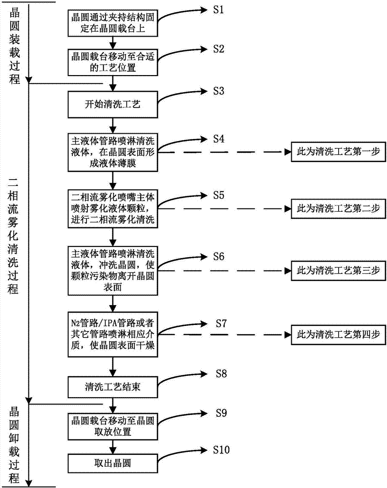
[0027] The core idea of ​​the present invention is: a kind of method of the present invention adopts two-phase flow atomization to clean wafer surface pollutant, realizes through the following steps:

[0028] Step 1: Make the wafer rotate at the first speed, spray the first cleaning liquid with the first flow rate on the surface of the wafer through the main liquid pipeline, so as to form a liquid film on the surface of the wafer, and perform a first-time cleaning on the surface of the wafer. cleaning;

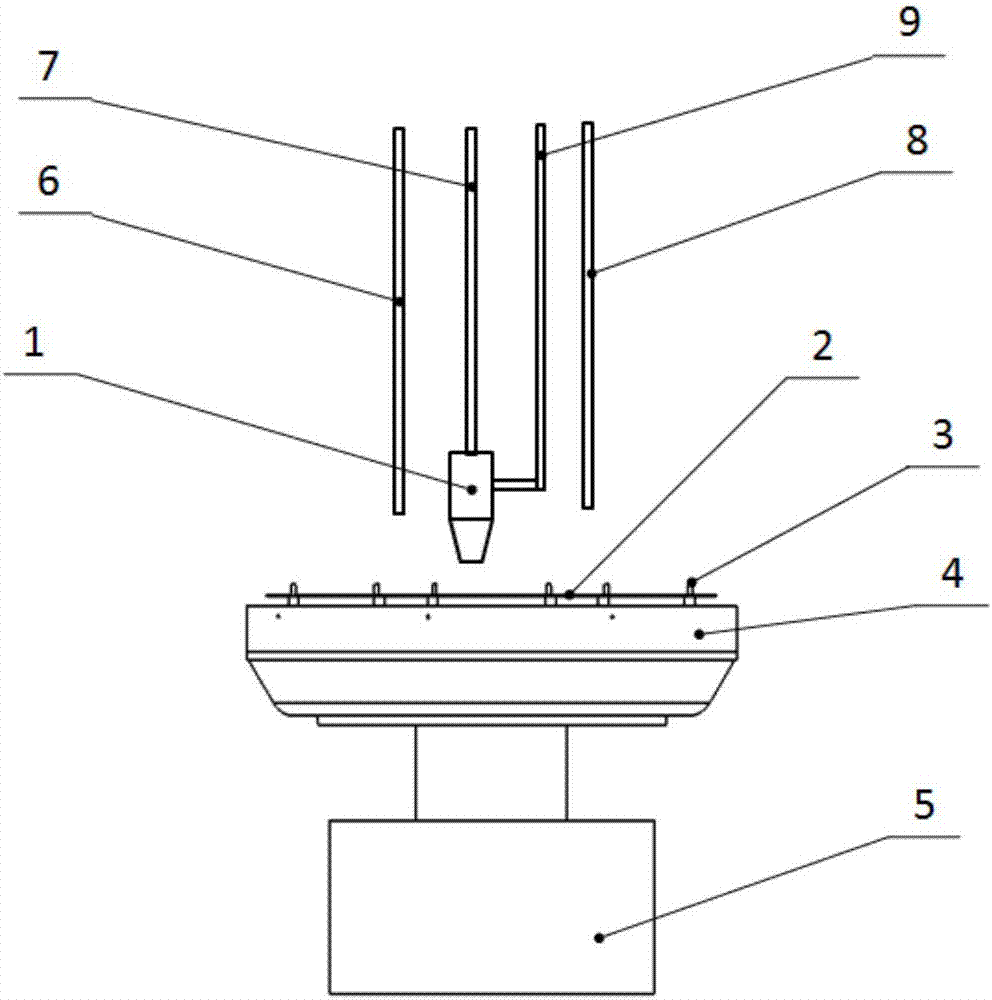
[0029] Step 2: Make the wafer rotate at the second speed, close the main liquid pipeline, and pass the second flow rate of gaseous cleaning medium and the third flow rate of liquid cleaning medium into the two-phase flow atomizing nozzle to pass the two-phase flow The atomizing nozzle sprays the modulated atomized liquid particles to the surface of the wafer, and performs two-phase flow atomization cleaning on the surface of the wafer at a second time;

[0030] Step 3: Make t...


PUM


Abstract

The invention discloses a method for cleaning surface contaminants of a wafer through twin-fluid atomization. The step process of the cleaning technology and the technological parameters used in all the steps are optimized, the technological conditions for cleaning the surface particle contaminants of the wafer through twin-fluid atomization are reasonably selected, and a cleaning technology window is clear so that effective cleaning of the surface of the wafer can be realized, the high removing efficiency of the particle contaminants can be guaranteed, the graphic structure on the surface of the wafer is not damaged and thus the integrated and optimized cleaning effect can be obtained.

Description

technical field [0001] The invention relates to the technical field of wet cleaning, and more specifically, to a method for removing pollutants on the surface of a wafer by means of two-phase flow atomization cleaning. Background technique [0002] The cleaning process is the most common process step in the integrated circuit manufacturing process, and its purpose is to effectively control the contamination level of each step to achieve the goal of each process step. [0003] On single-chip wet cleaning equipment, the effect of the cleaning process can be significantly improved by using gas-liquid two-phase atomization cleaning. During the atomization cleaning process, the atomized particles formed by the gas-liquid two-phase have an impact force on the liquid film covering the wafer surface, and form a rapidly propagating shock wave in the liquid film. When the shock wave acts on the particle pollutants , can speed up the detachment process of pollutants from the wafer sur...

Claims


Application Information

Patent Timeline
IPC IPC(8): H01L21/02
CPCH01L21/02H01L21/02057
Inventor 滕宇惠世鹏
Owner BEIJING SEVENSTAR ELECTRONICS CO LTD
Learn More