Wet cleaning method to eliminate copper corrosion

Inactive Publication Date: 2005-06-23
TAIWAN SEMICON MFG CO LTD
View PDF7 Cites 6 Cited by
  • Summary
  • Abstract
  • Description
  • Claims
  • Application Information

AI Technical Summary

Benefits of technology

[0006] To address the aforementioned shortcomings of conventional technology and in view of its purposes, the present invention provides a method for effectively

Problems solved by technology

A shortcoming of the use of copper is that copper is susceptible to corrosion when exposed to the environment.
The phenomenon of copper corrosion could result during these cleaning operations or subsequent to the cleaning operations as a result of the condition of the substr

Method used


Image

  • Wet cleaning method to eliminate copper corrosion

Examples


Embodiment Construction

[0012] The present invention provides a semiconductor substrate cleaning method that prevents copper corrosion. The cleaning method includes a DI (deionized) water cleaning operation in which the semiconductor substrate, alternatively referred to as a “wafer”, is rotated at a speed of no greater than 350 rpm. As will be discussed, the cleaning method of the present invention may include multiple distinct cleaning operations or steps.

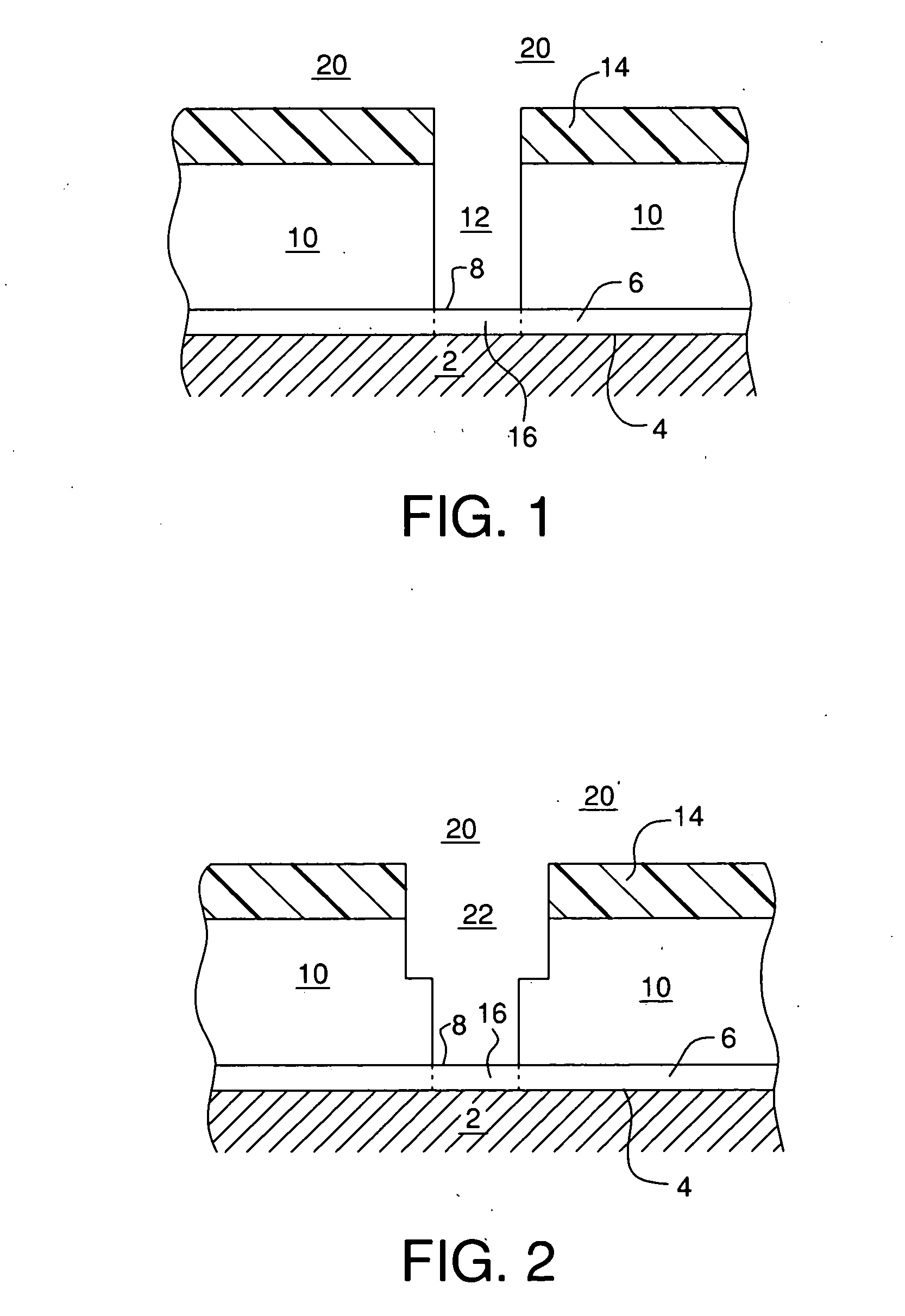
[0013] The wafer cleaning method of the present invention may be used at various stages during the formation of semiconductor devices on the wafer. A particularly advantageous application of the present invention is a cleaning operation used to clean a wafer with a copper-containing conductive material formed thereon and a film directly interposed between the copper containing conductive material and the environment. Such a structure may be produced after an etching operation. FIGS. 1 and 2 are each cross-sectional views of exemplary conventional struct...


PUM

PropertyMeasurementUnit
Diameteraaaaaaaaaa
Diameteraaaaaaaaaa
Angular velocityaaaaaaaaaa

Abstract

A method for cleaning semiconductor substrates includes a DI water clean operation that uses a spin speed no greater than 350 rpm. The cleaning method may include additional cleaning operations such as an organic clean, an aqueous chemical clean or a DI water/ozone clean. The cleaning method may be used to clean substrates after the conclusion of an etching procedure which exposes a single film between a Cu-containing conductive material and the environment. The spin speed of the DI water clean operation prevents copper corrosion due to breakdown of the film that separates the Cu-containing conductive material from the environment.

Description

FIELD OF THE INVENTION [0001] The present invention relates, most generally, to the manufacture of semiconductor devices. More particularly, the present invention relates to a semiconductor substrate cleaning method that prevents copper corrosion. BACKGROUND [0002] Copper is favored as a conductive material used in interconnect features in advanced, high-speed semiconductor devices. Damascene and dual damascene interconnect technology is advantageously used to provide planarized interconnect structures in advanced semiconductor manufacturing technologies. In processing operations used to form damascene, dual damascene and other openings, a dielectric layer is etched to expose a protective layer or etch stop layer. The exposed layer may be disposed directly between a subjacent copper-containing conductive material and the environment. A shortcoming of the use of copper is that copper is susceptible to corrosion when exposed to the environment. [0003] Dielectric etching operations use...

Claims


Application Information

Patent Timeline
IPC IPC(8): H01L21/02H01L21/306H01L21/3213H01L21/768
CPCH01L21/02063H01L21/76807H01L21/02071
Inventor CHOU, CHUN-LILIN, YIH-ANNHUANG, YI-CHENCHEN, CHAO-CHENGTAO, HUN-JAN
Owner TAIWAN SEMICON MFG CO LTD
Why Eureka
Try Eureka