Substrate processing device

A substrate processing device and technology for substrates, which are applied in the directions of transportation and packaging, cleaning flexible items, lighting and heating equipment, etc., can solve the problems of reduced cleaning ability, thick cleaning liquid L thickness, and reduced cleaning pressure, etc. The effect of cost reduction, effective cleaning process, and shortening of the conveying path

Inactive Publication Date: 2008-07-16
TOKYO ELECTRON LTD
View PDF1 Cites 7 Cited by
  • Summary
  • Abstract
  • Description
  • Claims
  • Application Information

AI Technical Summary

Problems solved by technology

[0009] However, in the conventional advection method, the cleaning liquid L is sprayed from the cleaning nozzle to the LCD substrate G in a horizontal position, as shown in FIG. Possibility that the thickness of cleaning liquid L on the substrate is too thick
[0010] That is, when the thickness of the cleaning liquid L on the substrate becomes thicker, the cleaning pressure of the cleaning liquid L sprayed from the cleaning nozzles 204, 206 on the substrate surface decreases, and at the same time, the new cleaning liquid cannot reach the substrate surface. , the problem of detergency of detergency
[0011] In addition, there is a problem that the cleaning solution supplied to the substrate remains on the substrate while containing foreign matter, and the foreign matter reattaches to the substrate G after the substrate drying process.
[0012] In addition, in order to prevent re-adhesion of such foreign matter, even if the cleaning time and the number of cleaning nozzles are increased, not only the transport path and processing time are increased, the throughput is reduced, but also the cost is increased.

Method used


Image

  • Substrate processing device
  • Substrate processing device
  • Substrate processing device

Examples


Embodiment Construction

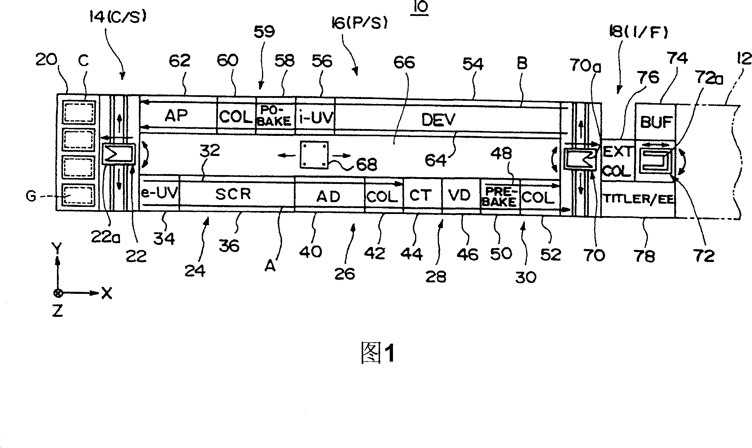
[0048] Embodiments of the present invention will be described below with reference to the drawings. FIG. 1 is a plan view of a coating and development processing system applicable to the substrate processing apparatus of the present invention.

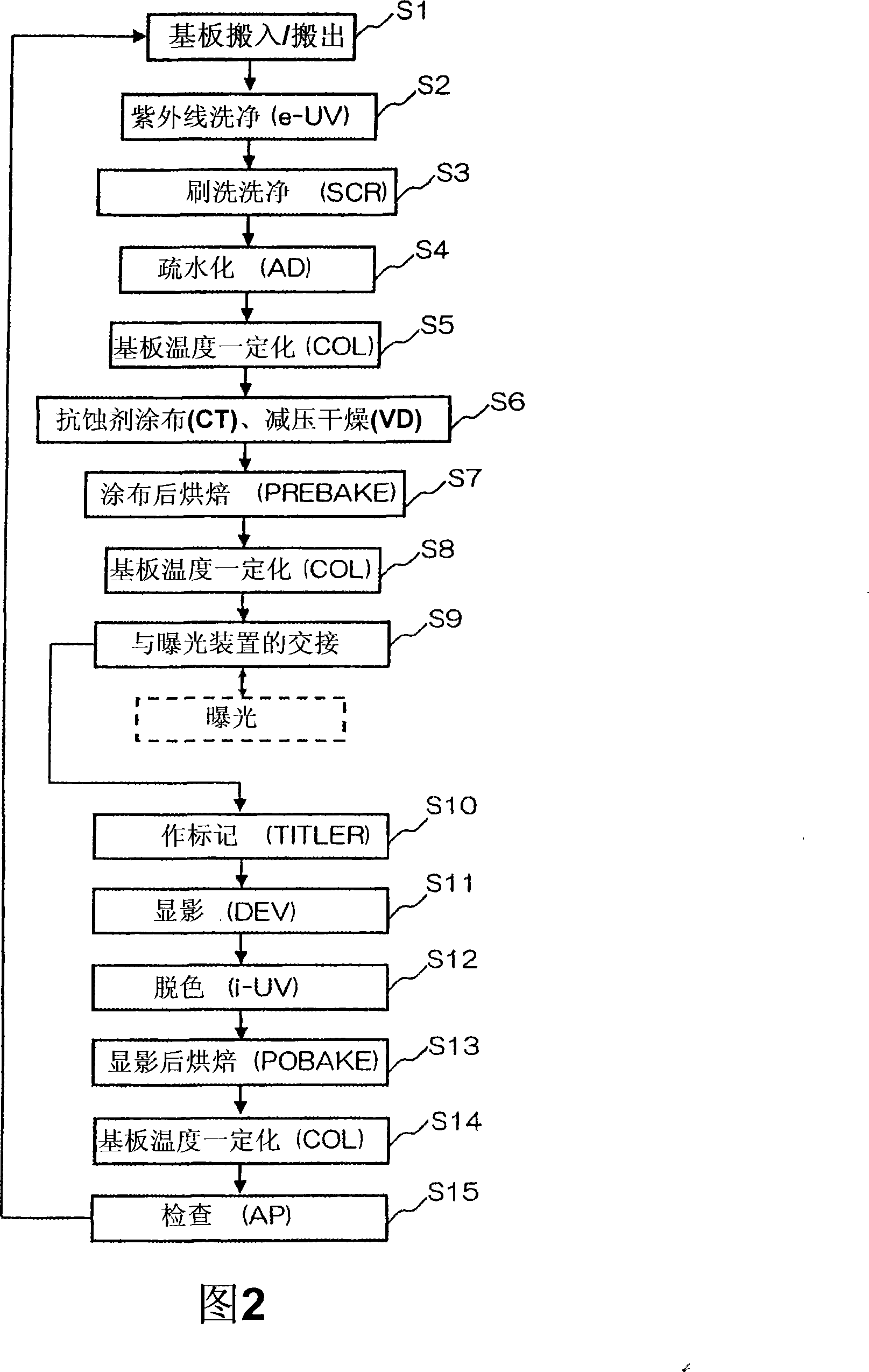
[0049] The coating and development processing system 10 is installed in a clean room, for example, a glass substrate for LCD is used as a substrate to be processed, and cleaning, resist coating, prebaking, developing and A series of processing such as post-baking. Exposure processing is performed in an external exposure device 12 provided adjacent to the system.

[0050] The coating and development processing system 10 is equipped with a horizontally long process station (processstation) (P / S) 16 at the center, and cassette stations (cassettestation) (C / S) 14 are arranged at both ends of its length direction (X direction). and interface station (I / F) 18 .

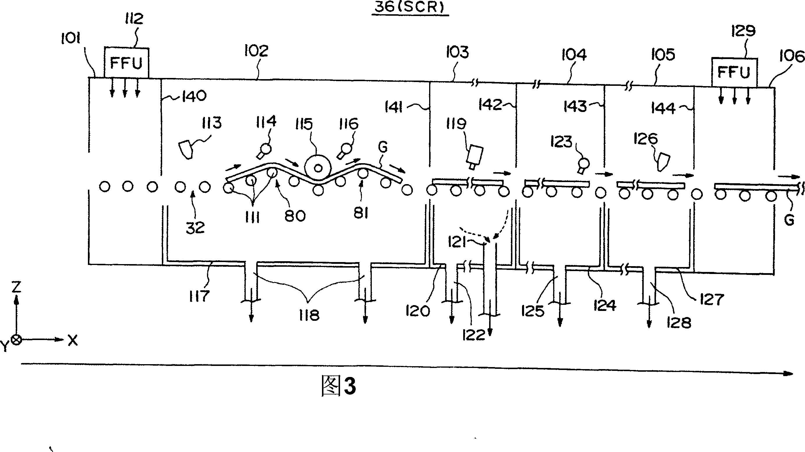
[0051] The cassette station (C / S) 14 has an aisle for loading and unloading ...


PUM


Abstract

The invention provides a substrate treating device which is used in a cleaning treatment of an untreated substrate to prevent a reattachment to the substrate for foreign bodies after a cleaning treatment, to effectively perform a cleaning treatment and to realize a increase of the production and a decrease of cost. The substrate treating device for cleaning the untreated substrate by using a cleaning liquid, comprises: a convey unit for conveying the substrate through a convey path formed for conveying the untreated substrate in a faceup manner; a cleaning nozzle for supplying the cleaning liquid to the conveyed substrate, wherein the convey path comprises a horizontal part for conveying the substrate in a horizontal state and an incline part which uptilts in a defined angle relative to the horizontal part; the cleaning nozzle is fixed above the incline part, the blowing direction of the cleaning nozzle falls towards a in a defined angle relative to the horizontal direction, and is an upstream direction of the convey path, and the nozzle blows the cleaning liquid to the inclination plane of the conveyed substrate on the incline part.

Description

technical field [0001] The present invention relates to a substrate processing apparatus for cleaning a substrate to be processed in a photolithography process. Background technique [0002] For example, in the manufacture of FPD (Flat Panel Display), after forming a predetermined film on the LCD substrate as the substrate to be processed, a photoresist (hereinafter referred to as resist) as a processing liquid is applied to form a resist film , Corresponding to the circuit pattern, the resist film is exposed, which is called development treatment, and the so-called photolithography process forms the circuit pattern. [0003] However, in a resist coating and development processing system that performs this photolithography process, a so-called advection method has been emphasized as a development method that can advantageously cope with an increase in the size of an LCD substrate. In this advection method, the LCD substrate is conveyed on a conveying path formed by conveyin...

Claims


Application Information

Patent Timeline
Patent Type & Authority Applications(China)
IPC IPC(8): B08B3/00B08B11/04B65G49/00B65G49/06B65G13/00G03F7/30G03F7/26H01L21/00H01L21/67H01L21/677
CPCH01L21/67028H01L21/67046H01L21/67051H01L21/67706
Inventor 坂井光广八寻俊一川内拓男小宫洋司
Owner TOKYO ELECTRON LTD
Why Eureka
Try Eureka