
Array substrate, liquid crystal display panel and display device

A technology for array substrates and base substrates, which is applied in the fields of instruments, nonlinear optics, optics, etc., can solve the problems of bad picture display, bridge structure can not be electrically connected to common electrodes, etc., and achieve the effect of reducing bad picture display

Active Publication Date: 2019-07-02
BOE TECH GRP CO LTD +1
View PDF7 Cites 0 Cited by
  • Summary
  • Abstract
  • Description
  • Claims
  • Application Information

AI Technical Summary

Problems solved by technology

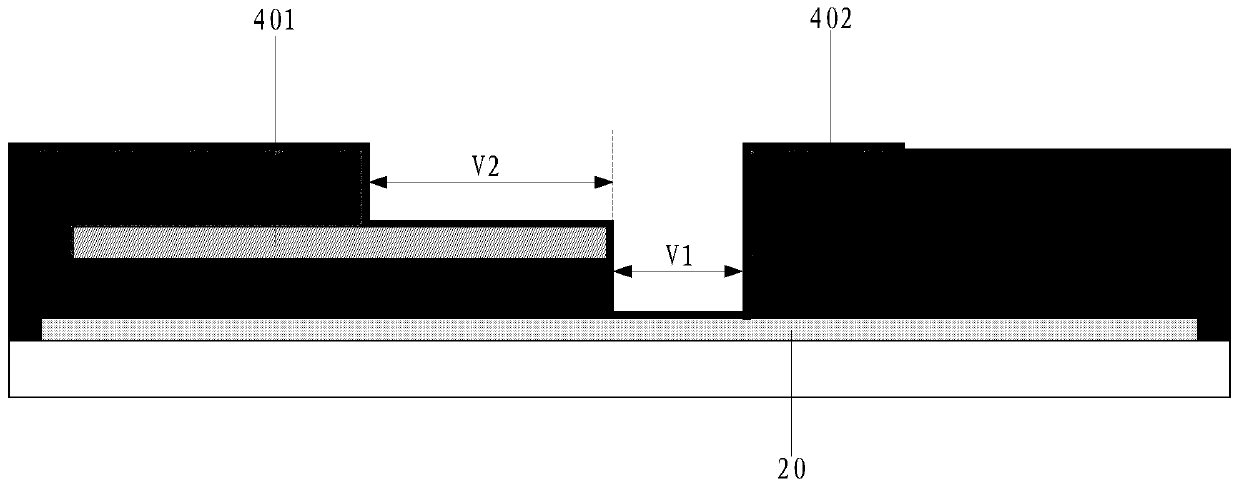
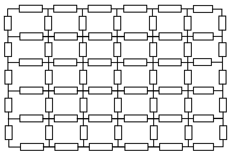
[0004] Therefore, ideally Figure 1a The equivalent circuit diagram of the common electrode 20 resistance in the shown structure is as follows Figure 1c shown; however, in the manufacturing process, it is impossible to completely overlap between different film layers, and there will be certain deviations. When there is a large deviation in the process, that is, a deviation in one direction, such as Figure 1d As shown, due to the small size of the deep hole region V1, it is easy to cover the deep hole region V1, so that the bridge structure cannot play the role of electrically connecting the common electrode. In this case, the equivalent resistance of the corresponding common electrode 20 is circuit diagram as Figure 1e As shown, the equivalent resistance of the common electrode 20 corresponding to two adjacent rows of pixels has a large difference, which leads to the problem of poor picture display

Method used


Image

  • Array substrate, liquid crystal display panel and display device
  • Array substrate, liquid crystal display panel and display device
  • Array substrate, liquid crystal display panel and display device

Examples


Embodiment Construction

[0029] In order to make the object, technical solution and advantages of the present invention clearer, the specific implementation of the array substrate provided by the embodiment of the present invention, its preparation method and liquid crystal display panel will be described in detail below with reference to the accompanying drawings.

[0030] The film thickness and shape of each layer in the drawings do not reflect the real scale of the array substrate, but are only intended to schematically illustrate the content of the present invention.

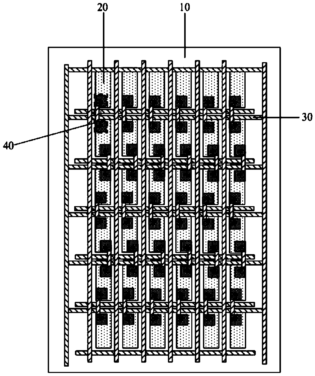
[0031] An embodiment of the present invention provides an array substrate, such as Figure 2a As shown, it includes: a base substrate 10, a plurality of common electrodes 20 arranged in a matrix on the base substrate 10; each common electrode 20 arranged along the first direction X passes through a common electrode line 30 extending along the first direction X direct contact to realize electrical connection; every two adjacent commo...


PUM


Abstract

The invention discloses an array substrate, a liquid crystal display panel and a display device. Every two adjacent common electrodes are electrically connected through a semi-through hole by adoption of a bridge connection structure; for each row of bridge connection structures which are arranged in the first direction, semi-through holes corresponding to one part of the bridge connection structures are first semi-through holes, and semi-through holes corresponding to the other part of the bridge connection structures are second semi-through holes. In this way, even if technological deviation exists in the first direction in a manufacturing process, a part of common electrodes in each row can achieve electrical connection through the bridge connection structures, and then equivalent resistances corresponding to random two adjacent common electrodes are consistent, and the problem that image display is poor can be solved.

Description

technical field [0001] The invention relates to the field of display technology, in particular to an array substrate, a liquid crystal display panel and a display device. Background technique [0002] Good picture quality is an essential feature of the display screen, but when displaying, the common electrode will be affected by the coupling capacitance between the gate line and the data line, resulting in the instability of the common electrode signal, which will bring afterimages to the display screen , Greenish, Crosstalk and other undesirable phenomena. [0003] The current solution to the instability of the common electrode signal can be achieved by reducing the coupling capacitance, such as Figure 1a As shown, the common electrode layer is cut into a plurality of common electrodes 20 with a block structure, and the common electrodes 20 arranged in the row direction are electrically connected by direct contact with the common electrode lines 30 extending in the row dir...

Claims


Application Information

Patent Timeline
Patent Type & Authority Patents(China)
IPC IPC(8): G02F1/1345
CPCG02F1/13452
Inventor 江鹏芮洲杨成绍
Owner BOE TECH GRP CO LTD
Learn More