Array substrate gate driving circuit, display panel and display device

A gate drive circuit, array substrate technology, applied in the direction of static indicators, instruments, etc., can solve the problems of inability to achieve the effect of TFT tube compensation, floating state fluctuations, and the inability to accurately predict the situation of applying the forward voltage of TFT tubes, etc. , to achieve the effect of ensuring normal display and improving reliability

Active Publication Date: 2017-07-04
BOE TECH GRP CO LTD
View PDF5 Cites 3 Cited by
  • Summary
  • Abstract
  • Description
  • Claims
  • Application Information

AI Technical Summary

Problems solved by technology

[0002] In some display panels, a strikethrough line in each row of GOA (Gate driver On Array, array substrate row driving technology) will be kept in a high state, so that the TFT (Thin Film Transistor, thin film transistor) in the corresponding pixel unit ) tube applies a forward voltage,

Method used


Image

  • Array substrate gate driving circuit, display panel and display device
  • Array substrate gate driving circuit, display panel and display device
  • Array substrate gate driving circuit, display panel and display device

Examples


Example Embodiment

[0030] The embodiments of the present invention will be described in detail below. Examples of the embodiments are shown in the accompanying drawings, wherein the same or similar reference numerals indicate the same or similar elements or elements with the same or similar functions. The embodiments described below with reference to the accompanying drawings are exemplary, and are intended to explain the present invention, but should not be construed as limiting the present invention.

[0031] The following describes the array substrate gate driving circuit, the display panel, and the display device according to the embodiments of the present invention with reference to the accompanying drawings.
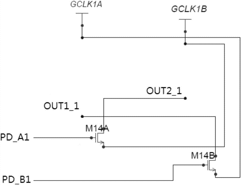
[0032] figure 1 It is a schematic structural diagram of a gate driving circuit of an array substrate according to an embodiment of the present invention.

[0033] In an embodiment of the present invention, the array substrate gate driving circuit includes: a first pull-down node PD_A1, a se...


PUM


Abstract

The invention discloses an array substrate gate driving circuit, a display panel and a display device. The driving circuit comprises a first transistor and a second transistor, wherein a control electrode of the first transistor is connected with a first pull-down node, a first electrode of the first transistor is connected with a second grid signal output terminal, and a second electrode of the first transistor is connected with a second clock signal terminal; a control electrode of the second transistor is connected with a second pull-down node, a first electrode of the second transistor is connected with a first grid signal output terminal, and a second electrode of the second transistor is connected with a first clock signal terminal; the first transistor is used for outputting a second clock signal to the second grid signal output terminal so as to enable the second grid signal output terminal to keep high-level signals at a non-selected output stage; the second transistor is used for outputting a first clock signal to the first grid signal output terminal so as to enable the first grid signal output terminal to keep high-level signals at a non-selected output stage. Thus, the problem that high-level signal fluctuation occurs at the non-selected output stages is effectively avoided.

Description

technical field [0001] The present invention relates to the field of display technology, in particular to an array substrate gate drive circuit, a display panel and a display device. Background technique [0002] In some display panels, a strikethrough line in each row of GOA (Gate driver On Array, array substrate row driving technology) will be kept in a high state, so that the TFT (Thin Film Transistor, thin film transistor) in the corresponding pixel unit ) tube applies a forward voltage, but because the GOA is in a floating state when outputting a high-level signal, the floating state will be fluctuated by other voltage changes, so it is impossible to accurately predict the forward voltage applied to the TFT tube, and thus cannot achieve The effect of TFT tube compensation. Contents of the invention [0003] The present invention aims to solve one of the technical problems in the related art at least to a certain extent. For this reason, the first object of the prese...

Claims


Application Information

Patent Timeline
IPC IPC(8): G09G3/20
CPCG09G3/20G09G2310/0267
Inventor 姚星郑皓亮商广良韩明夫韩承佑袁丽君王志冲金志河
Owner BOE TECH GRP CO LTD
Why Eureka
Try Eureka