Method and device for detecting surface defect of electronic device

A technology for electronic devices and defects, applied in the field of appearance inspection of electronic devices, can solve the problems of difficulty in inspection, eye fatigue, missed inspection and false inspection, and achieve the effects of shortening inspection time, improving production efficiency and high inspection efficiency.

Active Publication Date: 2017-07-07
GREE ELECTRIC APPLIANCES INC +1
View PDF5 Cites 29 Cited by
  • Summary
  • Abstract
  • Description
  • Claims
  • Application Information

AI Technical Summary

Problems solved by technology

At present, the detection of appearance defects of electronic devices including solder capacitors is still done by human eyes. It is difficult to detect relatively small defects, and the human eyes are tired for a long time, so the reliability and efficiency of the detection results are low. And it is prone to problems such as missed detection and false detection

Method used


Image

  • Method and device for detecting surface defect of electronic device
  • Method and device for detecting surface defect of electronic device
  • Method and device for detecting surface defect of electronic device

Examples


Embodiment Construction

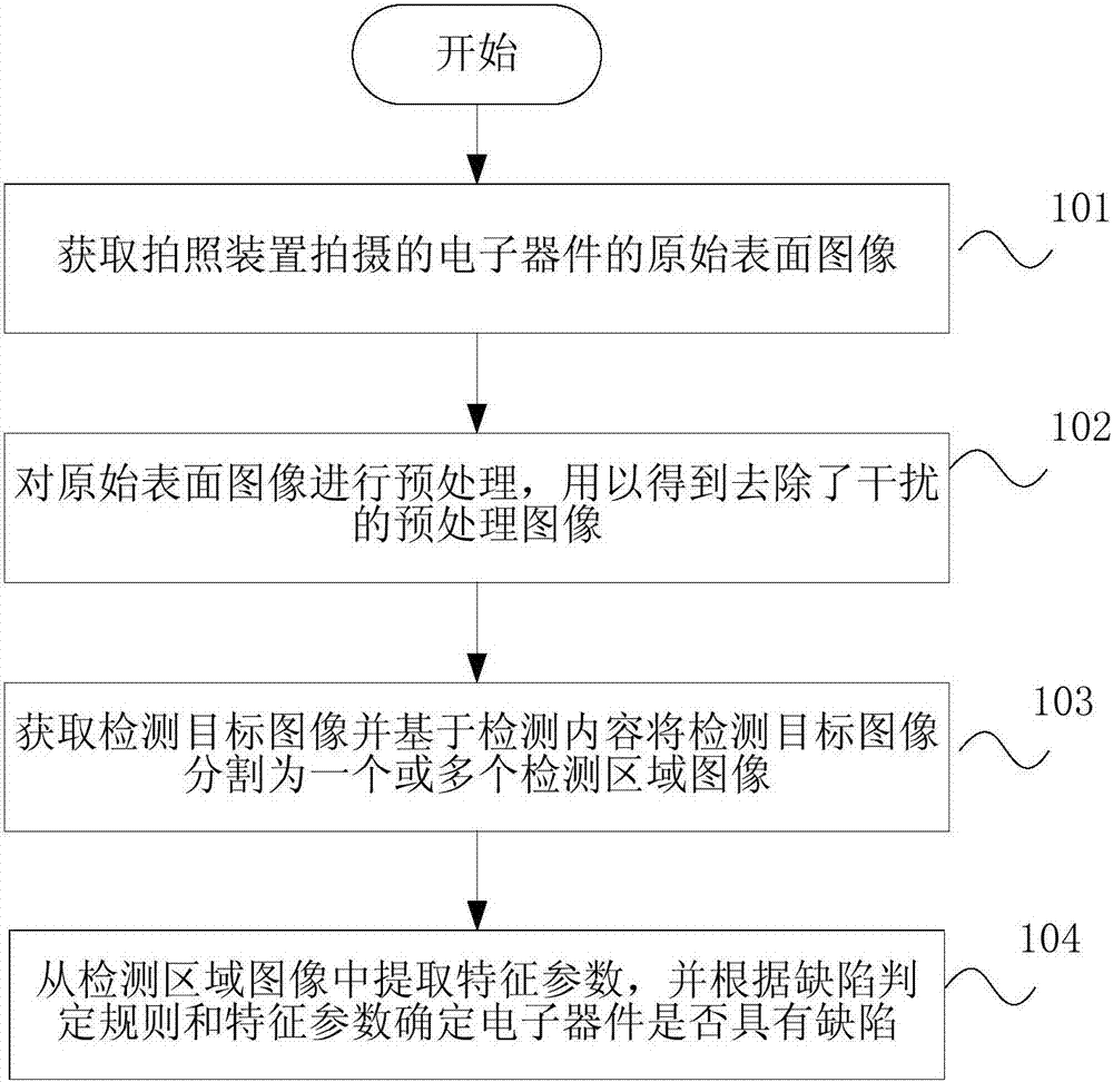
[0050] The present invention will be described more fully hereinafter with reference to the accompanying drawings, in which exemplary embodiments of the invention are illustrated. The following will clearly and completely describe the technical solutions in the embodiments of the present invention with reference to the accompanying drawings in the embodiments of the present invention. Obviously, the described embodiments are only some, not all, embodiments of the present invention. Based on the embodiments of the present invention, all other embodiments obtained by persons of ordinary skill in the art without making creative efforts belong to the protection scope of the present invention. The technical solution of the present invention will be described in various aspects below in conjunction with various figures and embodiments.

[0051] The "first", "second" and so on in the following are only used to describe the difference, and have no other special meanings.
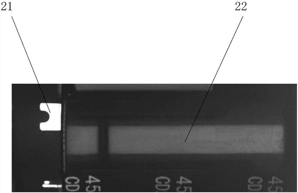
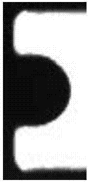
[0052] fi...


PUM


Abstract

The invention discloses a method and device for detecting a surface defect of an electronic device, relating to the field of electronic device appearance detection. The method comprises a step of obtaining an original surface image of an electronic device taken by a shooting device, a step of preprocessing the original surface image to obtain a preprocessed image with the removal of interference, a step of determining a detection target image in the preprocessed image and dividing the detection target image into one or more detection area images based on detection content, and a step of extracting a characteristic parameter from the detection area image, and determining whether the surface of the electronic device has a defect according to a defect judgment rule and the characteristic parameter. According to the method and device, the automatic detection of the surface defect of the electronic device can be realized, various defects can be detected at the same time, the shortcomings of the artificial detection of appearance defects are overcome, the detection efficiency is high, the misjudgment rate is low, the detection time can be shortened, and the production efficiency is improved.

Description

technical field [0001] The invention relates to the technical field of electronic device appearance detection, in particular to a method and device for detecting surface defects of electronic devices. Background technique [0002] With the development of industrial automation technology, the degree of automation of the production process is getting higher and higher. Electronic devices are widely used components, and their demand is increasing day by day. The appearance defects of various electronic devices, including solder capacitors, will lead to poor product performance and hidden dangers in product quality. Among them, taking solder tab capacitors as an example, in the actual production process of solder tab capacitors, defects such as flattening or protrusion of the aluminum shell, zooming or skewing of terminals will appear on the surface of the solder tab capacitor. In order to improve product quality, it is necessary to inspect the appearance of electronic devices...

Claims


Application Information

Patent Timeline
Patent Type & Authority Applications(China)
IPC IPC(8): G06T7/00G06T7/11G06T7/13
CPCG06T7/0004G06T2207/10004G06T2207/20024G06T2207/30108
Inventor 杨智慧
Owner GREE ELECTRIC APPLIANCES INC
Why Eureka
Try Eureka