

Display panel, display device and display panel manufacturing method
A technology for a display panel and a manufacturing method, which is applied in nonlinear optics, instruments, optics, etc., can solve the problems of low light transmittance of transparent display devices, many wiring designs on the first substrate, and poor transparent display effects, etc., to achieve Improve light transmittance, small thickness, and low production cost
- Summary
- Abstract
- Description
- Claims
- Application Information
AI Technical Summary
Problems solved by technology
Method used
Image

Examples
Embodiment Construction
[0051] In order to improve the light transmittance of the display device and improve the effect of transparent display, the embodiments of the present invention provide a display panel, a display device and a manufacturing method of the display panel. In order to make the purpose, technical solution and advantages of the present invention clearer, the following examples are given to further describe the present invention in detail.
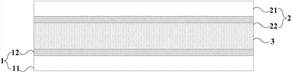
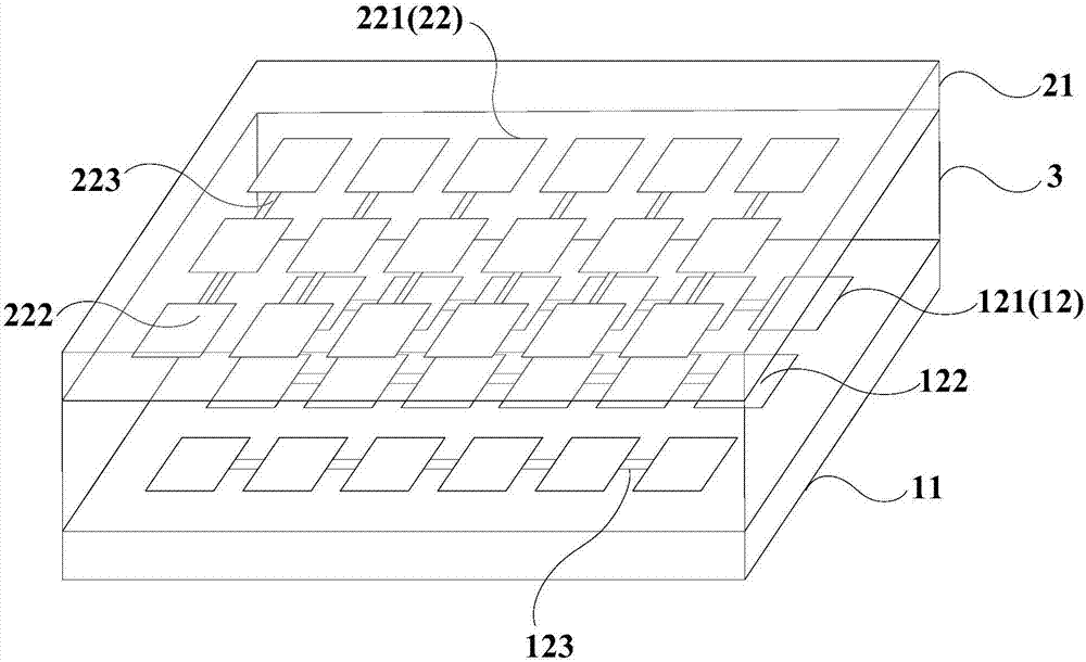
[0052] Such as figure 1 and figure 2 As shown, the embodiment of the present invention provides a display panel, including a first substrate 1 and a second substrate 2 oppositely arranged, and a liquid crystal layer 3 located between the first substrate 1 and the second substrate 2, wherein:
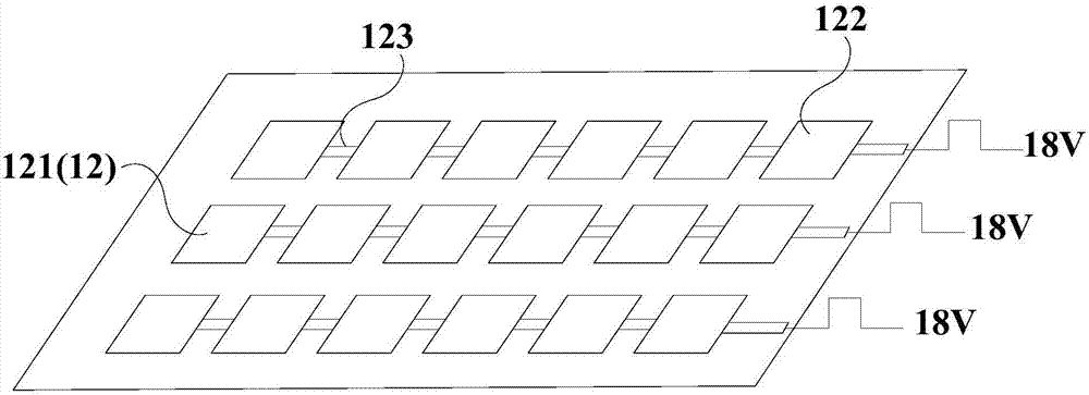
[0053] The first substrate 1 includes a first transparent base substrate 11, and a first transparent electrode layer 12 disposed on the side of the first transparent base substrate 11 close to the liquid crystal layer 3, the first transparent electrode lay...
PUM
| Property | Measurement | Unit |
|---|---|---|
| Thickness | aaaaa | aaaaa |
| Thickness | aaaaa | aaaaa |
Abstract
Description
Claims
Application Information