A display panel and a display device

A technology for display panels and display substrates, applied in instruments, nonlinear optics, optics, etc., can solve problems such as residual stress of display panels, and achieve the effect of reducing residual stress

Active Publication Date: 2020-05-29
BOE TECH GRP CO LTD +1
View PDF4 Cites 0 Cited by
  • Summary
  • Abstract
  • Description
  • Claims
  • Application Information

AI Technical Summary

Problems solved by technology

[0005] The purpose of the present invention is to solve the problem of residual stress in the existing display panel during the box alignment process

Method used


Image

  • A display panel and a display device
  • A display panel and a display device
  • A display panel and a display device

Examples


Embodiment Construction

[0030] In order to make the technical problems, technical solutions and advantages to be solved by the present invention clearer, the following will describe in detail with reference to the drawings and specific embodiments.

[0031] The present invention provides a solution to the problem of residual stress after box alignment in the prior art due to the uneven thickness of the film layer of the substrate.

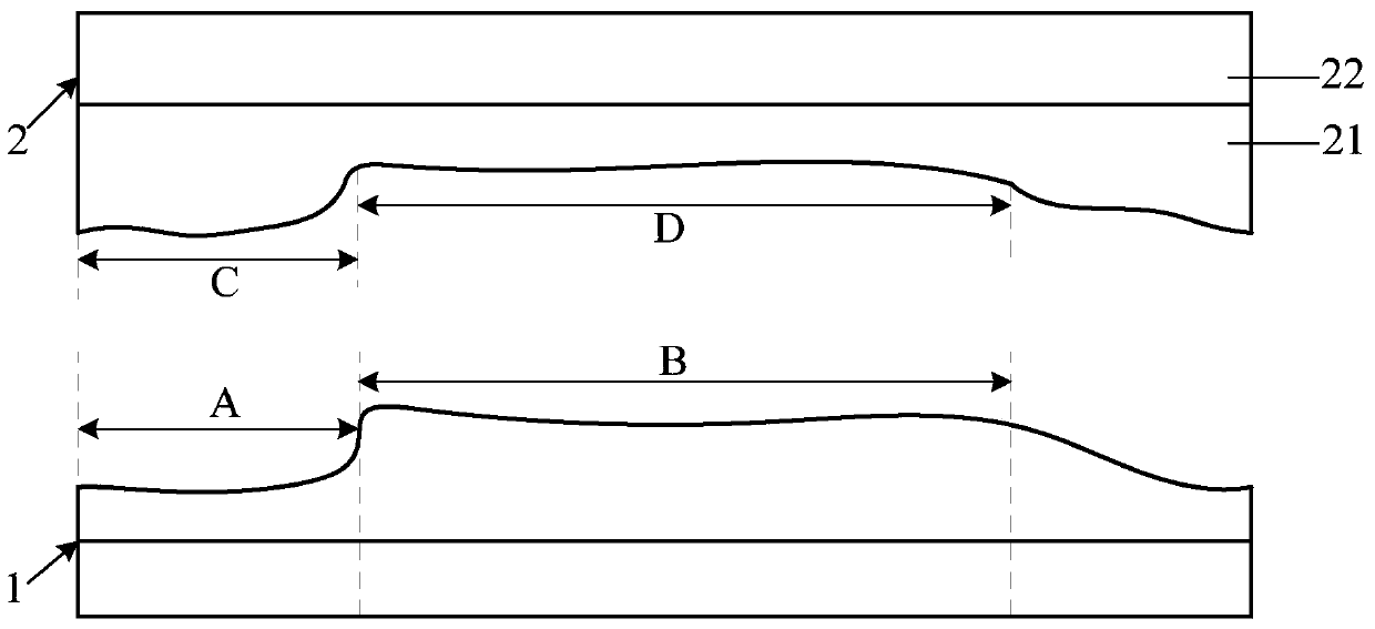
[0032] On the one hand, the embodiment of the present invention also provides a display panel, such as figure 1 As shown, it includes a display substrate 1 and a box-matching substrate 2 arranged in a box-to-box arrangement. Wherein, the display substrate 1 has at least a first part A and a second part B with different thicknesses formed on the side facing the box substrate 2 , the thickness of the first part A on the display substrate 1 is smaller than the thickness of the second part B on the display substrate 1 . That is to say, the display substrate 1 has the problem...


PUM

PropertyMeasurementUnit
thicknessaaaaaaaaaa

Abstract

The invention provides a display panel and a display device. The display panel comprises a pairing substrate and a display substrate which are arranged in pair, wherein a first part and a second part which are different in thickness are at least formed on the side, facing the pairing substrate, of the display substrate; the thickness of the first part on the display substrate is larger than that of the second part on the display substrate; the pairing substrate comprises a lining substrate and a pairing functional layer formed on the lining substrate; the pairing functional layer comprises a third part and a fourth part which are different in thickness; the thickness of the third part is smaller than that of the fourth part; after the pairing substrate and the display substrate are paired, forward projection of the third part on the display substrate and forward projection of the first part on the display substrate partially superpose, and forward projection of the fourth part on the display substrate and forward projection of the second part on the display substrate partially superpose. According to the scheme, remaining stress caused after the pairing substrate and the display substrate are paired can be reduced.

Description

technical field [0001] The present invention relates to the manufacturing field of display devices, in particular to a display panel and a display device. Background technique [0002] Currently, a display panel in a display device is formed by boxing an upper substrate and a lower substrate. During the manufacturing process, Marks (marks) for positioning are placed on some specific areas on the substrate. [0003] When making functional layers on the substrate, it is necessary to avoid these marks. Therefore, after the substrate is fabricated, the thickness of the film layer is often not guaranteed to be uniform. stress. Under the action of stress, the upper and lower substrates are prone to deformation. If the stress is not released before the sealant is cured, the deformation will remain, which will lead to uneven distance between the display panel boxes and affect the liquid crystal display. Often when the screen is displayed , the phenomenon of yellowing around the sc...

Claims


Application Information

Patent Timeline
Patent Type & Authority Patents(China)
IPC IPC(8): G02F1/1339
CPCG02F1/1339
Inventor 王国华钟国强任文明曹诚英
Owner BOE TECH GRP CO LTD
Why Eureka
Try Eureka