AlInGaN-based green and yellow light-emitting diode epitaxial structure

A technology of light-emitting diodes and epitaxial structures, which is applied in the direction of electrical components, circuits, semiconductor devices, etc., can solve the problems of V-pit 4 to enhance hole injection, etc., and achieve the effect of enhancing hole injection function and improving luminous efficiency

Active Publication Date: 2017-08-18
NANCHANG UNIV +1
View PDF6 Cites 9 Cited by
  • Summary
  • Abstract
  • Description
  • Claims
  • Application Information

AI Technical Summary

Problems solved by technology

Although this random distribution does not affect the function of V-pit 4 to shield d

Method used


Image

  • AlInGaN-based green and yellow light-emitting diode epitaxial structure
  • AlInGaN-based green and yellow light-emitting diode epitaxial structure
  • AlInGaN-based green and yellow light-emitting diode epitaxial structure

Examples


Embodiment 1

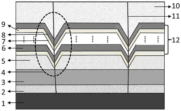
[0036] This embodiment introduces the epitaxial structure in which the starting position of the V-pit is the substrate.

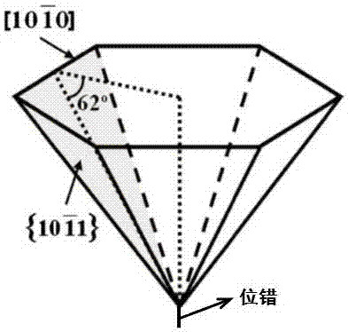
[0037] refer to Figure 5 . In the figure, 1 is the substrate, and the "process V-pit" 4 is periodically arranged on the substrate 1, and the schematic diagram of the projection of the "process V-pit" 4 on the upper surface of the substrate 1 is as follows Figure 4 shown. The buffer layer 2 is grown on the substrate 1. Due to the existence of the "process V pit" 4 on the substrate 1, a semipolar buffer layer 2 will also grow on the sidewall of the "process V pit" 4; moreover, the buffer layer 2 The growth rate on the semipolar face is less than that on the polar face. Therefore, a "process V-pit" 4 is also formed in the buffer layer 2, the size of which is larger than that of the "process V-pit" 4 in the substrate 1, and the periodic arrangement of the "process V-pit" 4 of the substrate 1 is inherited. . Similarly, growing the N-type AlInGaN layer 3 o...

Embodiment 2

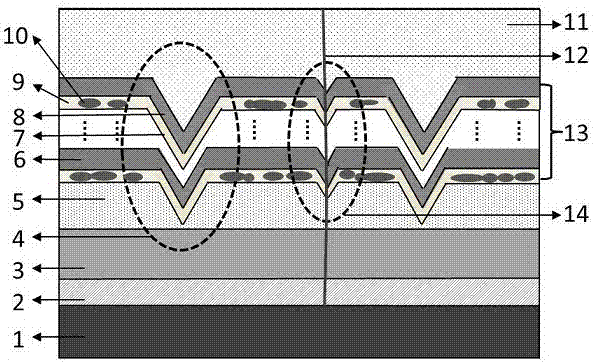
[0039] Compared with Example 1, the substrate 1 is changed to have no "process V-pit" 4 structure, that is, the "process V-pit" 4 starts in the buffer layer 2; the epitaxial structure refers to Figure 6 . In this epitaxial structure, the "process V-pit" 4 needs to be introduced after the buffer layer 2 is grown. Therefore, the entire epitaxial structure needs to be completed by means of secondary epitaxy.

Embodiment 3

[0041] Compared with Example 2, the buffer layer 2 is changed to have no "process V-pit" 4 structure, that is, the "process V-pit" 4 starts in the N-type AlInGaN layer 3; the epitaxial structure refers to Figure 7 . The epitaxial structure needs to grow the N-type AlInGaN layer 3 before introducing the "process V-pit" 4, so a secondary epitaxial method is required to complete the entire epitaxial structure.


PUM


Abstract

The invention discloses an AlInGaN-based green and yellow light-emitting diode (LED) epitaxial structure, which comprise a substrate for material growth and an AlInGaN-based semiconductor lamination layer stacked up on the semiconductor, wherein the AlInGaN-based semiconductor lamination layer at least comprises an N-type layer, a P-type layer and AlInGaN multiple quantum wells arranged between the N-type layer and the P-type layer. The structure is characterized in that the multiple quantum wells are embedded by V-shaped pits in periodic arrangement in a growth plane, and such V-shaped pits are same in size; and the plane quantum wells have similar-quantum-dot structures, which become main light-emitting sources of the LED. The epitaxial structure has the following advantages: 1) the similar-quantum-dot structures in the multiple quantum wells reduces impact of dislocation; 2) the multiple quantum wells are embedded by the process V-shaped pits in periodic arrangement in the growth plane, thereby further enhancing the hole injection function of the V-shaped pits; and 3) optimization of enhancement of the hole injection function of the V-shaped pits can be realized, and luminous efficiency of the LED can be improved.

Description

technical field [0001] The invention relates to semiconductor materials, in particular to an epitaxial structure of AlInGaN-based green and yellow light emitting diodes. Background technique [0002] Aluminum indium gallium nitride (AlInGaN)-based light-emitting diodes (LEDs) have a wide range of uses and can be used in markets such as instrument work instructions, traffic lights, large-screen displays, and general lighting. At present, AlInGaN-based LEDs have achieved great success in the blue light band, but their luminous efficiency in longer wave bands such as green and yellow light is still low. The reason is that the In composition of InGaN / GaN multiple quantum wells in green and yellow LEDs is high. A high In composition will introduce two unfavorable factors: 1) The lattice mismatch between the well barriers increases, the compressive stress increases, the piezoelectric polarization effect increases, and the dislocations increase; 2) The In composition is not easily...

Claims


Application Information

Patent Timeline
IPC IPC(8): H01L33/00H01L33/06H01L33/22H01L33/24H01L33/32
CPCH01L33/0075H01L33/06H01L33/22H01L33/24H01L33/32
Inventor 全知觉陶喜霞徐龙权丁杰莫春兰张建立王小兰刘军林江风益
Owner NANCHANG UNIV
Why Eureka
Try Eureka