Touch substrate, manufacturing method for touch substrate, and touch display panel

A touch display panel and substrate technology, which is applied in the fields of instruments, electrical digital data processing, and data processing input/output processes, etc., can solve problems such as the inability to achieve borderless, the blind spot and borderless touch display panel, etc. , to achieve the effect of no blind spots and no borders

Inactive Publication Date: 2017-08-25
BOE TECH GRP CO LTD +1
View PDF5 Cites 21 Cited by
  • Summary
  • Abstract
  • Description
  • Claims
  • Application Information

AI Technical Summary

Problems solved by technology

However, in practical applications, it is found that the reduction of the line width of the signal traces will increase its resistance, and the phenomenon of resistance-capacitance delay (RC Delay) is more serious; the reduction of the line spacing of the signal traces 5 will cause The crosstalk is more serious
More importantly, the technical means of reducing the line width and line spacing of the signal traces 5 in the prior art can only reduce the size of the border to a certain extent, and it cannot achieve true borderless
[0007] It can be seen from the above that the touch display panel in the prior art cannot achieve no blind spots and no borders at the same time

Method used


Image

  • Touch substrate, manufacturing method for touch substrate, and touch display panel
  • Touch substrate, manufacturing method for touch substrate, and touch display panel
  • Touch substrate, manufacturing method for touch substrate, and touch display panel

Examples


Embodiment Construction

[0054] In order for those skilled in the art to better understand the technical solutions of the present invention, a touch substrate, a manufacturing method thereof, and a touch display panel provided by the present invention will be described in detail below with reference to the accompanying drawings.

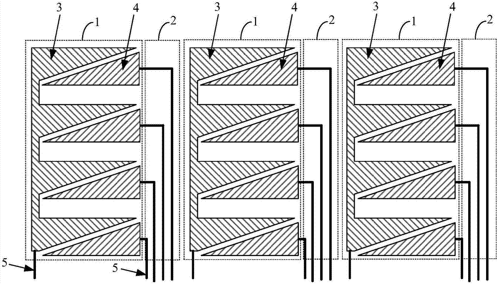
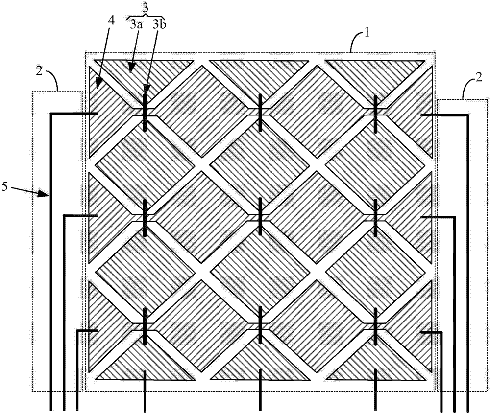
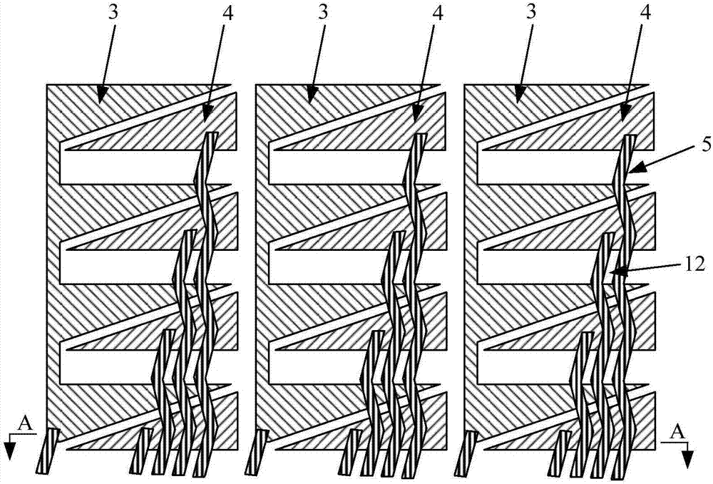
[0055] image 3 It is a schematic structural diagram of a touch substrate provided in Embodiment 1 of the present invention, Figure 4 for image 3 Schematic diagram of the cross-section in the direction of A-A, such as Figure 3 to Figure 4 As shown, the touch substrate includes: a base substrate 6 and a touch electrode layer located above the base substrate 6, and the touch electrode layer includes: a plurality of first touch electrodes 3 and a plurality of second touch electrodes 4, The first touch electrode 3 and the second touch electrode 4 are used to form a mutual capacitance. A first insulating layer 7 is arranged above the touch electrode layer, and the first insu...


PUM


Abstract

The invention discloses a touch substrate, a manufacturing method for the touch substrate, and a touch display panel. The touch substrate comprises a substrate and a touch electrode layer located above the substrate, wherein the touch electrode layer comprises first touch electrodes and second touch electrodes; a first insulation layer is arranged above the touch electrode layer; first via holes are formed in the first insulation layer; signal wires are arranged above the first insulation layer; and the signal wires are connected with the corresponding first or second touch electrodes through the first via holes. According to the technical scheme, the signal wires are arranged above the touch electrode layer, namely, wiring does not need to be performed in a peripheral region of the touch substrate, so that the finally formed touch display panel can be bezel-free; and meanwhile, the touch electrode layer can cover the whole substrate, so that no touch blind points exist on the touch substrate.

Description

technical field [0001] The invention relates to the field of display technology, in particular to a touch substrate, a preparation method thereof, and a touch display panel. Background technique [0002] With the improvement of user experience requirements for touch display devices, no blind spot and frameless design of touch display panels has become a current hot research topic in the field of touch display. [0003] figure 1 It is a schematic structural diagram of a single-layer multi-point external embedded touch display panel in the prior art, such as figure 1 As shown, the single layer multi-point embedded (Single Layer On-Cell, referred to as SLOC) touch display panel includes: alternately arranged touch area 1 and signal wiring area 2, wherein the touch area 1 is set There are several first touch electrodes 3 and several second touch electrodes 4, mutual capacitance is generated between the first touch electrodes 3 and the second touch electrodes 4; A plurality of...

Claims


Application Information

Patent Timeline
Patent Type & Authority Applications(China)
IPC IPC(8): G06F3/041
CPCG06F3/041G06F2203/04103G06F3/04164G06F3/0443G06F2203/04107G06F2203/04111G06F3/0445
Inventor 张绪杰郭总杰张明田健许世峰刘纯建
Owner BOE TECH GRP CO LTD
Why Eureka
Try Eureka