Array substrate, display panel and display device

An array substrate and display panel technology, applied in optics, instruments, electrical digital data processing, etc., can solve the problems of blue or purple display far away from the IC end, unevenness, etc.

An array substrate and display panel technology, applied in optics, instruments, electrical digital data processing, etc., can solve the problems of blue or purple display far away from the IC end, unevenness, etc.

CN107239172AInactive Publication Date: 2017-10-10BOE TECH GRP CO LTD +1

Image

  • Array substrate, display panel and display device
  • Array substrate, display panel and display device
  • Array substrate, display panel and display device

Examples


Embodiment Construction

[0029] The following will clearly and completely describe the technical solutions in the embodiments of the present invention with reference to the accompanying drawings in the embodiments of the present invention. Obviously, the described embodiments are only some, not all, embodiments of the present invention. Based on the embodiments of the present invention, all other embodiments obtained by persons of ordinary skill in the art without making creative efforts belong to the protection scope of the present invention.

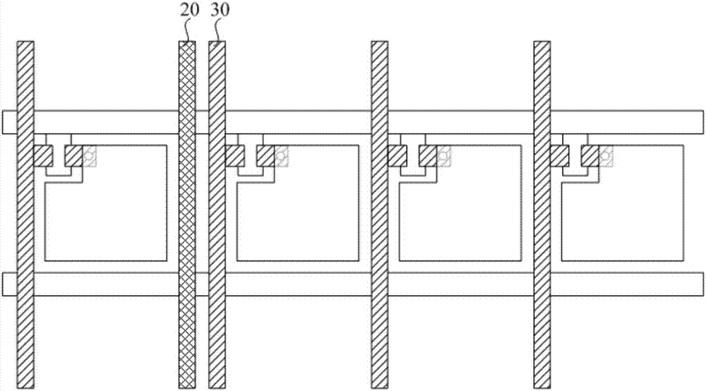
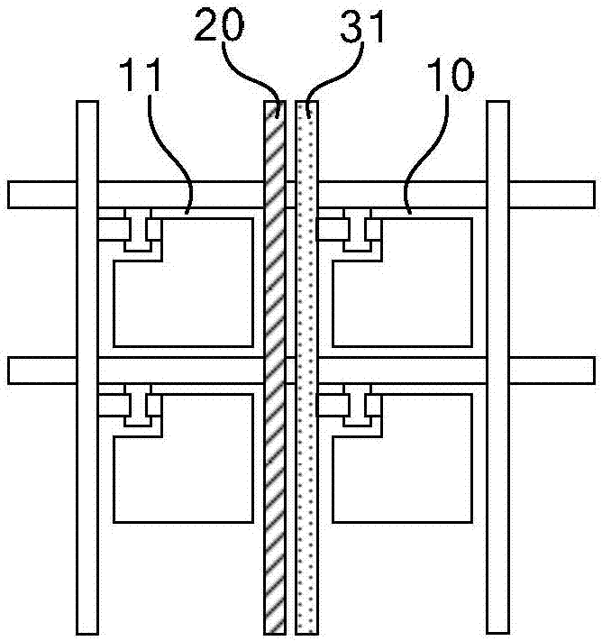
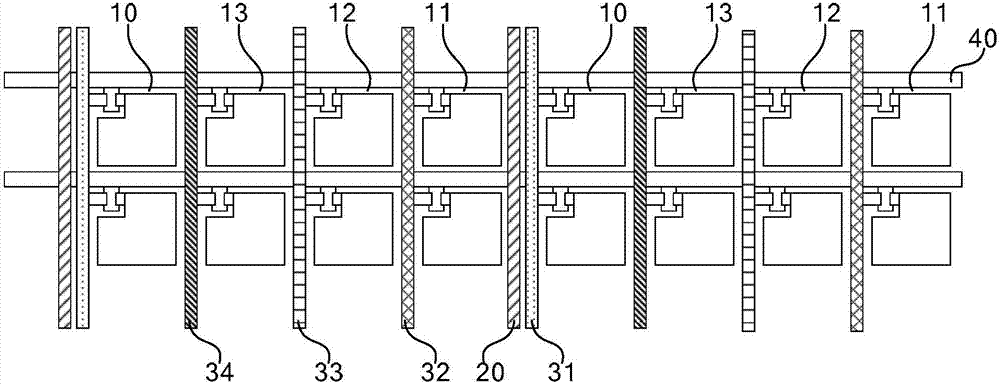
[0030] An embodiment of the present invention provides an array substrate, such as figure 2 As shown, it includes a white sub-pixel area 10 and a first color sub-pixel area 11 adjacent to the white sub-pixel area 10; a touch electrode line 20 is arranged between the white sub-pixel area 10 and the first color sub-pixel area 11; Wherein, at most a first data line 31 is provided between the white sub-pixel area 10 and the first color sub-pixel area 11 , and the...


PUM


Abstract

The embodiment of the invention provides an array substrate, a display panel and a display device, and relates to the technical field of display. According to the array substrate, the display panel and the display device, the problems of non-uniform display caused by signals on a touch electrode wire can be avoided. The array substrate comprises a white sub-pixel area and a first color sub-pixel area which is adjacent to the white sub-pixel area; the touch electrode wire is arranged between the white sub-pixel area and the first color sub-pixel area, wherein a first data line is at most arranged between the white sub-pixel area and the first color sub-pixel area, and the first data line is used for providing data signals for sub-pixel electrodes in the white sub-pixel area.

Description

technical field [0001] The present invention relates to the field of display technology, in particular to an array substrate, a display panel and a display device. Background technique [0002] With the rapid development of display technology, the birth of a touch panel (TP for short) makes people's lives more convenient. Today, the embedded capacitive touch technology has been widely used in the field of display technology. [0003] Wherein, in order to realize the touch function, touch electrode lines electrically connected to the touch electrodes must be provided, so as to input touch signals to the touch electrodes through the touch electrode lines, or receive sensing signals fed back by the touch electrodes. like figure 1 As shown, in the prior art, most products place the touch electrode lines 20 and the data lines 30 close to each other on the array substrate. [0004] However, such a design will cause the data signal on the data line 30 to be pulled or interfered ...

Claims


Application Information

Patent Timeline
10 Oct 2017
Publication
CN107239172A
IPC
G06F3/041; G02F1/1333
CPC
G02F1/13338; G06F3/0412; G02F1/136286; G02F2201/52; G06F2203/04105; G06F3/04164; G06F3/04166; G06F3/0446
Inventors
孙东领; 王立森