Flash memory cell, flash memory array and method of operation

A flash memory cell, flash memory array technology, applied in electrical components, information storage, read-only memory, etc., can solve the problem that the flash memory cell cannot be further reduced

Active Publication Date: 2020-07-31
SHANGHAI HUAHONG GRACE SEMICON MFG CORP
View PDF4 Cites 0 Cited by
  • Summary
  • Abstract
  • Description
  • Claims
  • Application Information

AI Technical Summary

Problems solved by technology

[0004] The object of the present invention is to provide a flash memory unit, a flash memory array and an operation method thereof, so as to solve the problems that the flash memory unit cannot be further reduced in the prior art.

Method used


Image

  • Flash memory cell, flash memory array and method of operation
  • Flash memory cell, flash memory array and method of operation

Examples


Embodiment Construction

[0030] The specific implementation manner of the present invention will be described in more detail below with reference to schematic diagrams. Advantages and features of the present invention will be apparent from the following description and claims. It should be noted that all the drawings are in a very simplified form and use imprecise scales, and are only used to facilitate and clearly assist the purpose of illustrating the embodiments of the present invention.

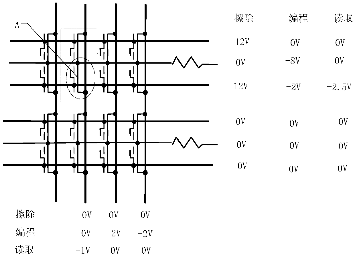
[0031] Usually, SST N-channel flash memory is programmed by hot electrons at the source, which requires a large overlapping area between the floating gate and the drain to provide a large enough coupling coefficient. The gate provides a large enough coupling voltage, but in this way, the large overlapping area of ​​the floating gate and the drain will not be conducive to the scaling of the flash memory.

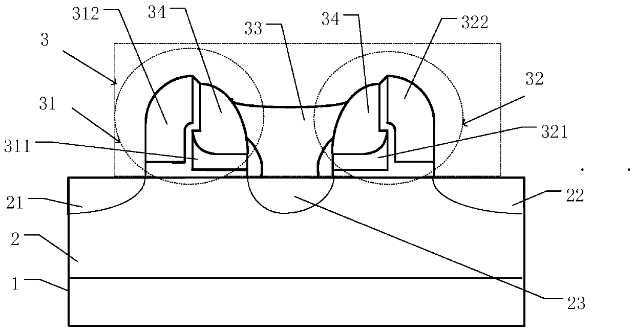
[0032] refer to figure 1 , which is a schematic diagram of the flash memory unit provided by the embodiment...


PUM


Abstract

The invention provides a flash memory unit, a flash memory array and an operation method thereof, comprising: an N well is formed in a P-type substrate, a P-type doped region is formed in the N well, and the P-type doped region is used as the first A source, a second source, and a drain; the gate structure on the N well is located between the first source and the second source, and the gate structure has a symmetric structure with respect to the source polysilicon Two storage bits, each containing a floating gate and a wordline gate. The flash memory unit provided by the present invention is programmed by generating high-energy electrons or even hot electrons through the collision ionization of hot holes at the pinch-off point of the drain, which is beneficial to the miniaturization of the device and achieves the purpose of reducing the unit area of ​​the device.

Description

technical field [0001] The invention relates to the field of semiconductor manufacturing, in particular to a flash memory unit, a flash memory array and an operation method thereof. Background technique [0002] As an integrated circuit storage device, flash memory (flash memory) is widely used in portable computers, mobile phones, digital music players, etc. devices and other electronic products. [0003] Generally speaking, when manufacturing flash memory, we must try our best to consider how to reduce the size and power consumption of each memory cell. However, the existing SST flash memory structure requires a large overlapping area between the floating gate and the drain through source-side hot electron programming. Provide a sufficiently large coupling coefficient, only in this way, the voltage applied to the source polysilicon during programming can provide a sufficiently large coupling voltage to the floating gate, but the disadvantages of this are: the large overla...

Claims


Application Information

Patent Timeline
Patent Type & Authority Patents(China)
IPC IPC(8): H01L27/11524G11C16/10G11C16/08
CPCG11C16/08G11C16/10H10B41/35
Inventor 徐涛
Owner SHANGHAI HUAHONG GRACE SEMICON MFG CORP
Why Eureka
Try Eureka