Memory, detection method thereof and chip

A memory and laser detection technology, applied in the field of memory, can solve the problems of high production cost and low detection accuracy of laser detectors, and achieve the effects of low production cost, small space occupation and improved accuracy

Active Publication Date: 2017-12-15
GIGADEVICE SEMICON (BEIJING) INC
View PDF5 Cites 2 Cited by
  • Summary
  • Abstract
  • Description
  • Claims
  • Application Information

AI Technical Summary

Problems solved by technology

[0005] Embodiments of the present invention provide a memory, its detection method, and a chip to solve the problems of low detection accuracy and high production cost of laser detectors integrated in existing chips

Method used


Image

  • Memory, detection method thereof and chip
  • Memory, detection method thereof and chip
  • Memory, detection method thereof and chip

Examples


Embodiment Construction

[0034] In order to make the purpose, technical solutions and advantages of the present invention clearer, the technical solutions of the present invention will be clearly and completely described through implementation with reference to the accompanying drawings in the embodiments of the present invention. Obviously, the described embodiments are the embodiment of the present invention. Some, but not all, embodiments. Based on the embodiments of the present invention, all other embodiments obtained by persons of ordinary skill in the art without making creative efforts belong to the protection scope of the present invention.

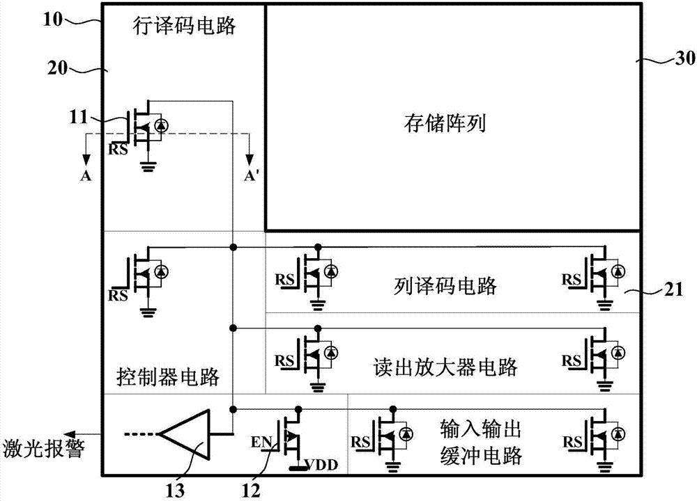
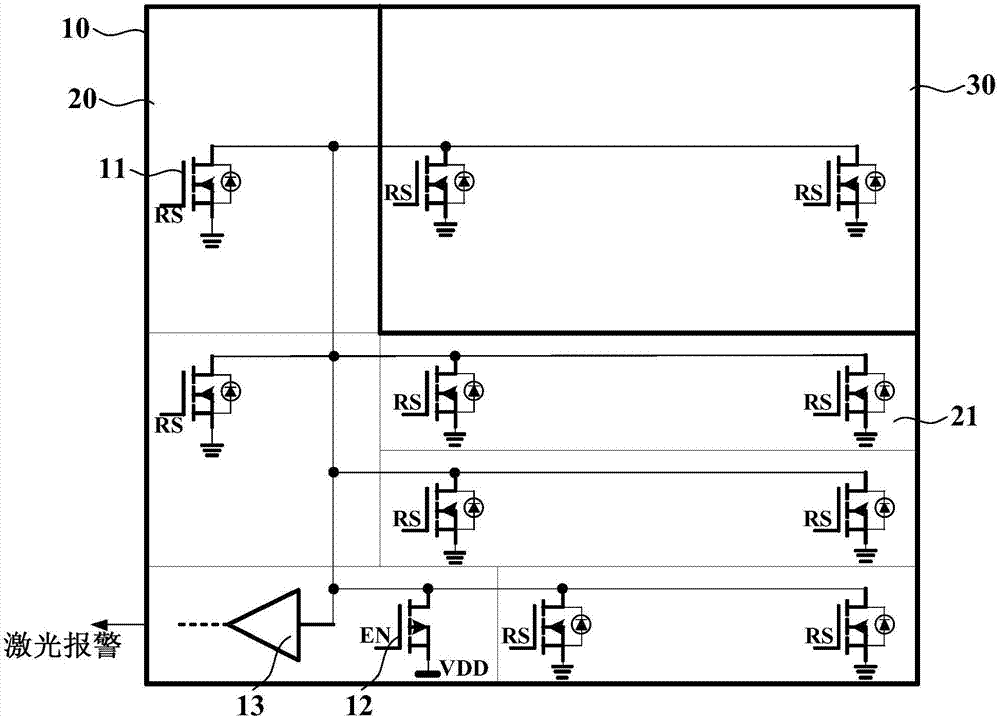
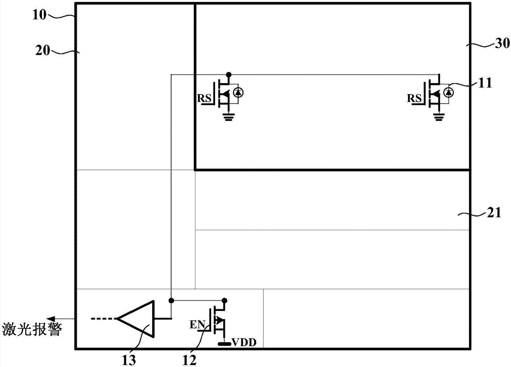
[0035] refer to Figure 1 ~ Figure 3 As shown, it is a schematic diagram of various memories provided by the embodiments of the present invention. The memory provided by the embodiments of the present invention can be integrated in various chips or circuits, and the optional memory type is any existing memory type, such as ROM, RAM, EEPROM, Flash, and th...


PUM


Abstract

The embodiment of the invention discloses a memory, a detection method thereof and a chip. The memory comprises a substrate, a laser detection circuit located on the substrate, as well as a data circuit region and a data memory region located on the substrate, wherein the laser detection circuit at least comprises a plurality of monitoring transistors, at least one charging transistor and at least one amplifier unit; an input terminal of the amplifier unit is electrically connected with an output terminal of the at least one monitoring transistor and the output terminal of the charging transistor respectively; the input terminal of the monitoring transistor is grounded; the input terminal of the charging transistor is electrically connected with a power supply; the data circuit region is provided with a plurality of sensitive circuits; the data memory region is provided with a memory array; each of the sensitive circuits is arranged adjacent to the at least one monitoring transistor; and/or the memory array is arranged adjacent to at least one monitoring transistor. The memory provided by the embodiments of the invention is low in production cost, can effectively improve laser detection accuracy, and can avoid detection leakage.

Description

technical field [0001] The embodiments of the present invention relate to memory technology, and in particular to a memory, a detection method thereof, and a chip integrated with the memory. Background technique [0002] In the field of information security applications, security chips based on specific cryptographic algorithms need to provide information security protection for internal sensitive information and protect the confidentiality and integrity of information. Due to the importance of its internal information, the security chip will also be attacked in various forms, and is facing serious security challenges. [0003] At present, it is a common method for hackers to crack chips by using exception injection attack means to obtain keys, and one of the effective exception injection attack means is laser fault injection attack means. The basic principle of the laser fault injection attack method to attack the chip is the internal photoelectric effect. The laser is usu...

Claims


Application Information

Patent Timeline
Patent Type & Authority Applications(China)
IPC IPC(8): G11C29/12
CPCG11C29/12
Inventor 朱磊
Owner GIGADEVICE SEMICON (BEIJING) INC
Why Eureka
Try Eureka