Array substrate and liquid crystal display and driving method thereof

A technology of an array substrate and a driving method, applied in the field of liquid crystal display, capable of solving problems such as flickering and uneven display of images, achieving the effects of improving display quality, improving display unevenness and flickering

Active Publication Date: 2017-12-22
KUSN INFOVISION OPTOELECTRONICS
View PDF6 Cites 24 Cited by
  • Summary
  • Abstract
  • Description
  • Claims
  • Application Information

AI Technical Summary

Problems solved by technology

[0008] The object of the present invention is to provide an array substrate, a liquid crystal display device and a driving method, which can realize switching between wide and narrow viewing angles in different occasions, and improve the problems of uneven display and flickering of the screen

Method used


Image

  • Array substrate and liquid crystal display and driving method thereof
  • Array substrate and liquid crystal display and driving method thereof
  • Array substrate and liquid crystal display and driving method thereof

Examples


no. 1 example

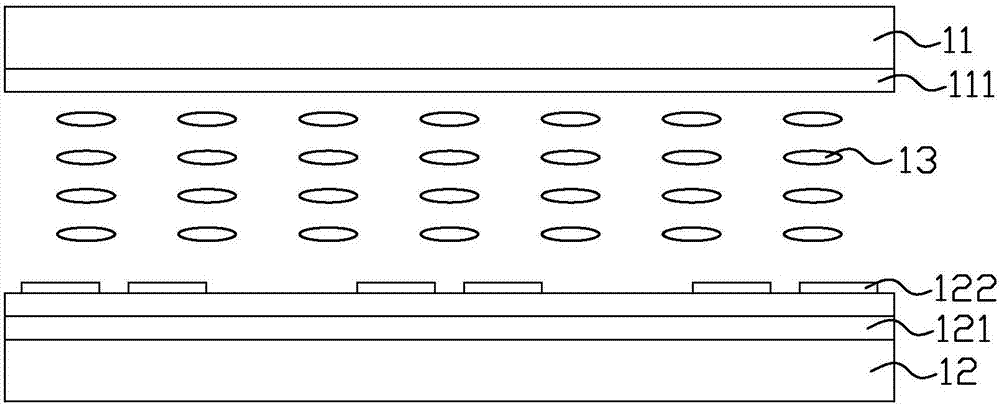
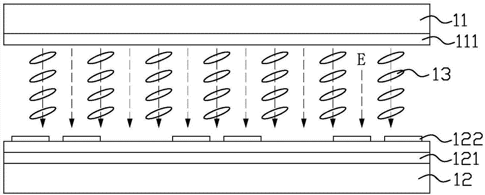
[0037] Please refer to Figure 5 to Figure 7 The liquid crystal display device provided by the first embodiment of the present invention includes a display panel 50, and the display panel 50 includes an array substrate 20, a color filter substrate 30 disposed opposite to the array substrate 20, and a color filter substrate located between the array substrate 20 and the color filter substrate 30. Liquid crystal layer 40 .

[0038] A plurality of scan lines 21 and a plurality of data lines 22 are disposed on the array substrate 20 . The plurality of scan lines 21 and the plurality of data lines 22 are insulated and intersect to define a plurality of pixel units arranged in an array. Each pixel unit is provided with a pixel electrode 23 and a thin film transistor 26 , and the pixel electrode 23 is connected to the scanning line 21 and the data line 22 adjacent to the thin film transistor 26 through the thin film transistor 26 . Specifically, the thin film transistor 26 includes...

no. 2 example

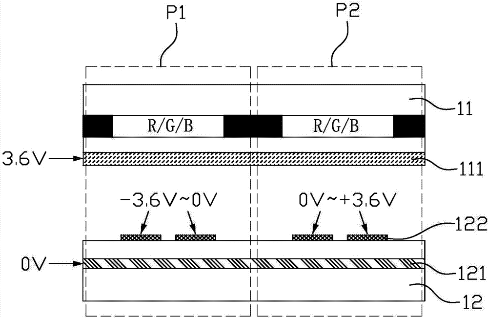
[0065] Please refer to Figure 13 The difference between the liquid crystal display device provided in this embodiment and the above-mentioned first embodiment is that in this embodiment, the plurality of first common electrode strips 24a and the plurality of second common electrode strips 24b are arranged in the direction of the data line 22 The way of setting them apart from each other is: in the direction of the data line 22, every two first common electrode strips 24a and every two second common electrode strips 24b are alternately arranged, that is, the pixel units in the first and second rows are composed of the first The common electrode strips 24a cover the pixel units in the third and fourth rows are covered by the second common electrode strips 24b, and so on, and the above arrangement is repeated every four subsequent rows.

[0066] For other structures of this embodiment, reference may be made to the foregoing first embodiment, and details are not repeated here.

no. 3 example

[0068] Please refer to Figure 14 The difference between the liquid crystal display device provided in this embodiment and the above-mentioned first embodiment is that in this embodiment, each pixel unit in each row is connected to the same scanning line 21 and is controlled by the same scanning line 21 , the common electrode strips 24 of each row are connected to the scanning lines 21 controlling the pixel units of the row through corresponding control switches 25 . For example, each pixel unit in the first row is connected to the scanning line Gate0 on the upper side of the pixel unit in the row, and the common electrode strip 24a in the first row is connected to the scanning line Gate0 controlling the pixel unit in the row through the control switch 25a ; Each pixel unit in the second row is connected to the scanning line Gate1 on the upper side of the pixel unit in the row, and the common electrode strip 24b in the second row is connected to the scanning line Gate1 control...


PUM


Abstract

The invention discloses an array substrate and a liquid crystal display and a driving method thereof. Multiple scanning lines, multiple data lines and multiple pixel units in array configuration are arranged on the array substrate, the array substrate is further provided with a first voltage line, a second voltage line, multiple common electrode strips and multiple control switches, each common electrode strip extends in the direction of the scanning lines, the common electrode strips consist of multiple first common electrode strips and multiple second common electrode strips, the multiple first common electrode strips and the multiple second common electrode strips are arranged alternately in the direction of the data lines, the multiple control switches consist of multiple first control switches and multiple second control switches, each first common electrode strip is connected with the first voltage line and the corresponding scanning line through the corresponding first control switch, and each second common electrode strip is connected with the second voltage line and the corresponding scanning line through the corresponding second control switch.

Description

technical field [0001] The invention relates to the technical field of liquid crystal display, in particular to an array substrate, a liquid crystal display device and a driving method. Background technique [0002] Liquid crystal display (liquid crystal display, LCD) has the advantages of good image quality, small size, light weight, low driving voltage, low power consumption, no radiation and relatively low manufacturing cost, and occupies a dominant position in the field of flat panel display. [0003] With the continuous advancement of liquid crystal display technology, the viewing angle of the display has been expanded from about 120° to more than 160°. While enjoying the visual experience brought by the large viewing angle, people also hope to effectively protect commercial secrets and personal privacy. Avoid commercial loss or embarrassment caused by information leakage on the screen. Therefore, in addition to a wide viewing angle, it is also required that the displa...

Claims


Application Information

Patent Timeline
Patent Type & Authority Applications(China)
IPC IPC(8): G02F1/1343G02F1/1362G09G3/36
CPCG02F1/134363G02F1/136286G09G3/3614G09G3/3696G02F1/134381
Inventor 乔艳冰赵哲朱欢欢
Owner KUSN INFOVISION OPTOELECTRONICS
Why Eureka
Try Eureka