Array substrate, display panel and display device

A technology for array substrates and display areas, applied in optics, instruments, electrical components, etc., can solve the problems of large non-display area width and unfavorable narrow borders

Active Publication Date: 2018-01-09
XIAMEN TIANMA MICRO ELECTRONICS
View PDF8 Cites 46 Cited by
  • Summary
  • Abstract
  • Description
  • Claims
  • Application Information

AI Technical Summary

Problems solved by technology

[0004] Embodiments of the present invention provide an array substrate, a display panel, and a display device, which are used to solve the problem in the prior art that the non-display area of ​​the array substrate has a large width and is not conducive to narrow borders

Method used


Image

  • Array substrate, display panel and display device
  • Array substrate, display panel and display device
  • Array substrate, display panel and display device

Examples


Embodiment Construction

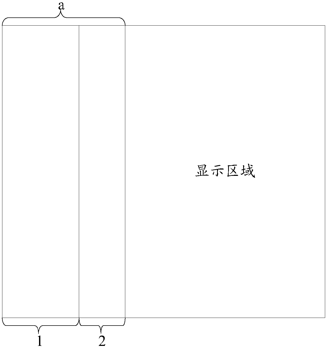
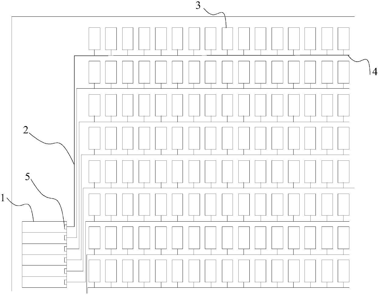
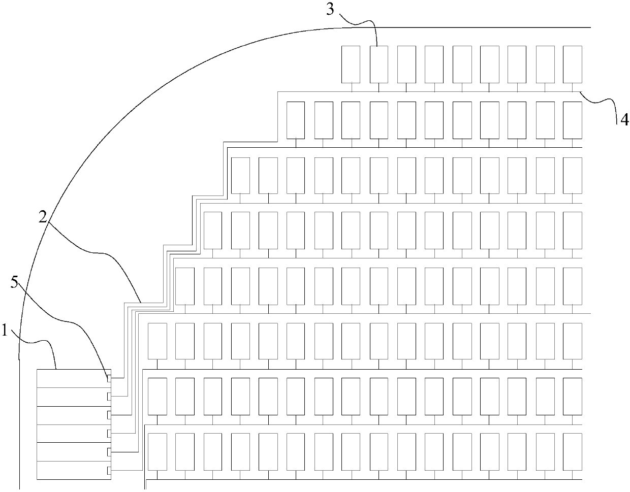
[0061] At present, in the existing array substrate, at the non-display area on one side such as the left frame, such as Figure 1a The schematic structural diagram of the array substrate in the prior art shown generally includes elements such as a gate driving circuit 1 and a gate fan-out wiring 2 . Moreover, at the left border, from the display area to the direction of the outer edge, the gate fan-out wiring 2 and the gate driving circuit 1 are sequentially and continuously arranged. Specifically, such as Figure 1b The schematic diagram of the structure of the array substrate in the prior art shown at right-angled corners, the gate lines 4 connected to the pixels 3 in the display area need to be connected to the corresponding signal output in the gate drive circuit 1 through the connected gate fan-out lines 2 terminal 5, wherein the signal output terminal 5 is disposed on the side of the gate drive circuit 1 close to the display area. Therefore, generally the total width a ...


PUM


Abstract

The invention discloses an array substrate, a display panel and a display device. A grid-electrode driving circuit and a plurality of grid-electrode fan wires which are positioned in a non-display area separately and a plurality of grid lines positioned in a display area are involved; one end of each grid-electrode fan wire is electronically connected with the corresponding signal output end of the grid-electrode driving circuit, and the other end of each grid-electrode fan wire is electrically connected with the corresponding grid line. By arranging an overlapping area between first grid-electrode wires in the gird-electrode fan wires and the grid-electrode driving circuit outside a mutual electrical connection area, a certain overlapping area is located between the area where the grid-electrode fan wires are located and the grid-electrode driving circuit, and therefore the occupied space of the first grid-electrode fan wires outside the grid-electrode driving circuit can be decreased, and the space between the grid-electrode driving circuit and the display area is reduced as much as possible, so that the width of the non-display area in the extension direction of the grid lines can be narrowed, and the bezel width of the display panel is reduced.

Description

technical field [0001] The present invention relates to the field of display technology, in particular to an array substrate, a display panel and a display device. Background technique [0002] At present, the screens of common display devices, such as monitors, televisions, mobile phones, tablet computers, etc., are usually regular rectangles. In order to improve the display effect of the display device, more and more people begin to pay attention to the narrow bezel design of the display device, especially for the splicing screen used for large-screen outdoor display, the narrow bezel display device can effectively reduce the splicing in the splicing screen. The width of the seam significantly improves the overall display effect. In the prior art, narrow bezel displays are usually produced by compressing the size of the components at the bezel, which not only limits the compression ratio, but also increases the process requirements, reduces the production yield, and at th...

Claims


Application Information

Patent Timeline
Patent Type & Authority Applications(China)
IPC IPC(8): G02F1/1362H01L27/32
CPCH01L27/1248G02F1/13452G02F2201/56H01L27/124G02F1/133388H10K59/131H01L27/1218
Inventor 赖国昌李俊谊张中杰
Owner XIAMEN TIANMA MICRO ELECTRONICS
Why Eureka
Try Eureka