A resistive memory and its manufacturing method

A technology of resistive variable memory and manufacturing method, which is applied in the direction of electrical components, etc., can solve the problem of a small number of storage units, and achieve the effect of increasing storage capacity

Active Publication Date: 2018-10-30
YANGTZE MEMORY TECH CO LTD
View PDF4 Cites 0 Cited by
  • Summary
  • Abstract
  • Description
  • Claims
  • Application Information

AI Technical Summary

Problems solved by technology

Existing RRAMs generally form a plurality of memory cells located on the same plane on a semiconductor substrate. For a substrate with a fixed area, the number of memory cells formed is relatively small.

Method used


Image

  • A resistive memory and its manufacturing method
  • A resistive memory and its manufacturing method
  • A resistive memory and its manufacturing method

Examples


Embodiment Construction

[0055] The following will clearly and completely describe the technical solutions in the embodiments of the present invention with reference to the accompanying drawings in the embodiments of the present invention. Obviously, the described embodiments are only some, not all, embodiments of the present invention. Based on the embodiments of the present invention, all other embodiments obtained by persons of ordinary skill in the art without making creative efforts belong to the protection scope of the present invention.

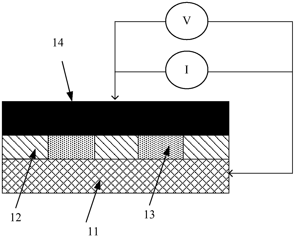
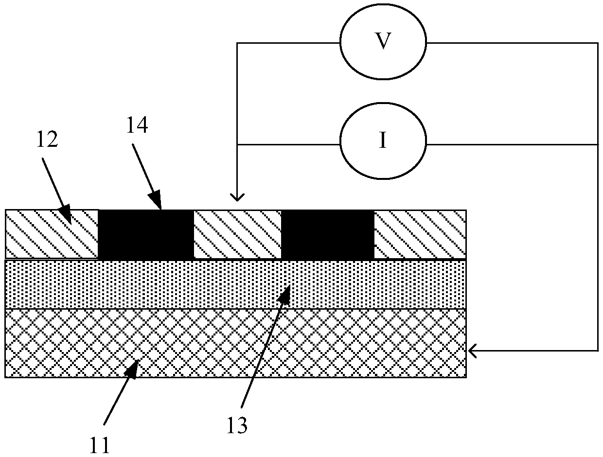
[0056] refer to figure 1 ,figure 1 It is a structural schematic diagram of a 2D resistive variable memory. A resistive variable medium layer 13 is formed on the surface of a semiconductor substrate 11. The resistive variable medium layer is divided into a plurality of storage units through the insulating medium layer 13. The storage units are located on the same plane and are connected as electrodes. 14 and the substrate 11 use the electrical characteristics o...


PUM


Abstract

The invention discloses a resistive random access memory and a production method thereof. The production method includes: providing a substrate; forming functional layers on the substrate in sequence,wherein the functional layers include multiple insulation layers and multiple resistive dielectric layers; forming a first trough penetrating the functional layers to have the functional layers divided into two parts, wherein the depth of the first trough is greater than the thickness of the functional layers and is smaller than the sum of the thickness of the functional layers and the substrate,and in the two parts of the functional layers, one ends of the resistive dielectric layers and facing to the first trough are first ends while one ends away from the first trough are second ends; forming first polar structures in the first trough connected with the first ends of the resistive dielectric layers; forming second polar structures on side faces and tops of the functional layers, wherein the second polar structures are connected with the second ends of the resistive dielectric layers. Multiple memory units can be formed on the substrate, and memory capacity is improved.

Description

technical field [0001] The present invention relates to the technical field of storage devices, and more specifically, relates to a resistive variable memory and a manufacturing method thereof. Background technique [0002] With the continuous development of science and technology, more and more electronic devices are applied to people's daily life and work, bringing great convenience to people's daily life and work, and becoming an indispensable tool for people today. [0003] Memory is an important component of many electronic devices. As the functions of electronic devices become more and more powerful, more and more data is required in the memory, and the memory capacity of the memory is required to be larger and larger. Resistive variable memory is a common type of memory. In conventional RRAMs, a plurality of memory cells located on the same plane are generally formed on a semiconductor substrate. For a substrate with a fixed area, the number of memory cells formed is...

Claims


Application Information

Patent Timeline
Patent Type & Authority Patents(China)
IPC IPC(8): H01L45/00
Inventor 张肖可王家友
Owner YANGTZE MEMORY TECH CO LTD
Why Eureka
Try Eureka