PCB inner layer pattern optimization method, PCB, board splicing structure and laminating structure

A technology of inner layer pattern and optimization method, applied in the field of electronics, can solve the problems of copper foil wrinkling and lack of glue, and achieve the effect of improving pressure loss and improving the uniformity of glue flow.

Inactive Publication Date: 2018-01-23
GUANGZHOU FASTPRINT CIRCUIT TECH +2
View PDF7 Cites 6 Cited by
  • Summary
  • Abstract
  • Description
  • Claims
  • Application Information

AI Technical Summary

Problems solved by technology

[0003] Based on this, the present invention is to overcome the defects of lack of glue and copper foil wrinkling in the copper-free ar...

Method used


Image

  • PCB inner layer pattern optimization method, PCB, board splicing structure and laminating structure
  • PCB inner layer pattern optimization method, PCB, board splicing structure and laminating structure
  • PCB inner layer pattern optimization method, PCB, board splicing structure and laminating structure

Examples


Embodiment Construction

[0032] In order to make the object, technical solution and advantages of the present invention clearer, the present invention will be further described in detail below in conjunction with the accompanying drawings and specific implementation methods. It should be understood that the specific embodiments described here are only used to explain the present invention, and do not limit the protection scope of the present invention.

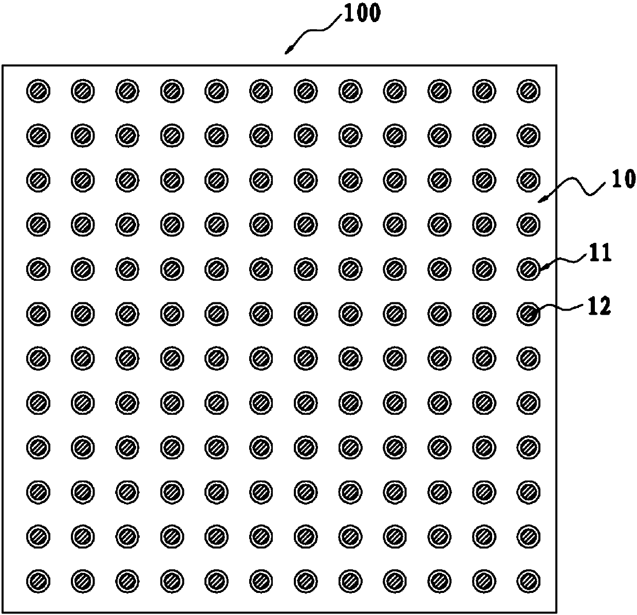
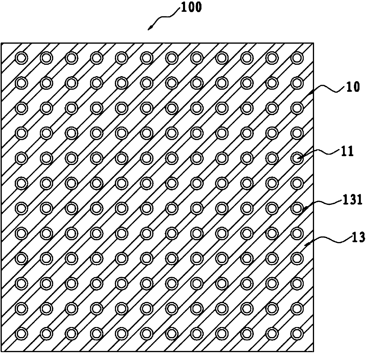
[0033] Such as figure 1 The optimization method of a kind of PCB inner layer pattern shown, PCB inner layer pattern includes copper area 600 and copper-free area 100, and described copper-free area 100 includes the via area 10 that is provided with at least one via hole 11, when there is When the remaining copper ratio of the copper area is less than a specific value, a copper point 12 is arranged at the via hole position of the via hole 11 , and the diameter of the copper point 12 is smaller than the diameter of the via hole.

[0034] Since there is...


PUM


Abstract

The invention discloses an optimization method for a PCB inner layer pattern, a PCB, a board splicing structure and a laminating structure. The PCB inner layer pattern comprises a coppery region and anon-copper region; the non-copper region comprises a via hole region with at least one via hole; and when a residual copper rate of the coppery region is smaller than a specific value, copper pointsare laid out at via hole positions of the via holes, and the diameter of each copper point is smaller than that of each via hole. Such small-size copper points laid out can improve uniformity of distribution of the pattern and reduce a volume of glue required for glue filling in the non-copper region, so that risks of wrinkling, cavities and the like of a copper foil subjected to lamination processing can be reduced, and meanwhile, the size of each copper point is smaller than that of each via hole, so that in the driving process, the copper points can be drilled off; and in addition, layout of the copper points can further promote PCB drilling quality to a certain degree and particularly has a great improvement effect on drilling haloing, so that CAF performance of the PCB is improved.

Description

technical field [0001] The invention relates to the field of electronics, and more specifically, to a method for optimizing inner layer graphics of a PCB, a PCB, a jigsaw structure and a laminated structure. Background technique [0002] Traditionally, with the rapid development of the electronics industry, the printed circuit board, which is an indispensable part of the electrical performance transmission of electronic products, is constantly tending to high-speed and high-layer development. High multi-layer circuit boards are made by multiple core boards and prepregs with lines and other graphics through lamination, drilling, electroplating, etching and other processes. Among them, lamination processing is one of the key processes in PCB production. PCB The quality of lamination is related to the further processing and application of subsequent products, such as drilling, graphics production, plug hole grinding, product reliability, PCB placement, etc. For high-multilayer...

Claims


Application Information

Patent Timeline
IPC IPC(8): H05K1/11H05K1/14
CPCH05K1/11H05K1/14
Inventor 程柳军陈蓓李艳国李华
Owner GUANGZHOU FASTPRINT CIRCUIT TECH
Why Eureka
Try Eureka