Display panel and display device

A technology for display panels and substrates, applied in semiconductor devices, electrical components, transistors, etc., to solve problems such as light leakage in dark states

Active Publication Date: 2018-01-30
WUHAN TIANMA MICRO ELECTRONICS CO LTD
View PDF3 Cites 2 Cited by
  • Summary
  • Abstract
  • Description
  • Claims
  • Application Information

AI Technical Summary

Problems solved by technology

[0004] The present invention provides a display panel and a display device to ...

Method used


Image

  • Display panel and display device
  • Display panel and display device
  • Display panel and display device

Examples


Embodiment Construction

[0025] In order to further explain the technical means and functions adopted by the present invention to achieve the intended purpose of the invention, the specific implementation, structure, and features of a display panel and a display device proposed according to the present invention will be described below in conjunction with the accompanying drawings and preferred embodiments. And its effect, detailed description is as follows.

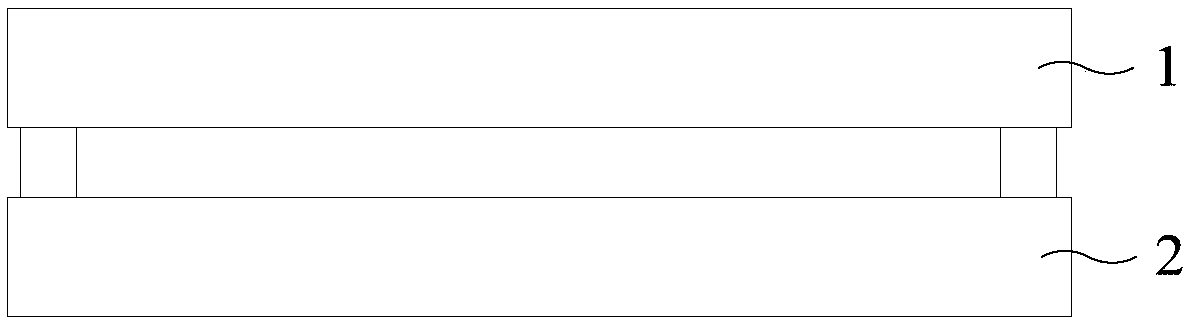
[0026] An embodiment of the present invention provides a display panel, and the display panel includes a first substrate and a second substrate oppositely arranged;

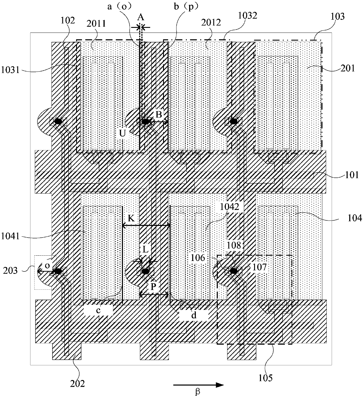
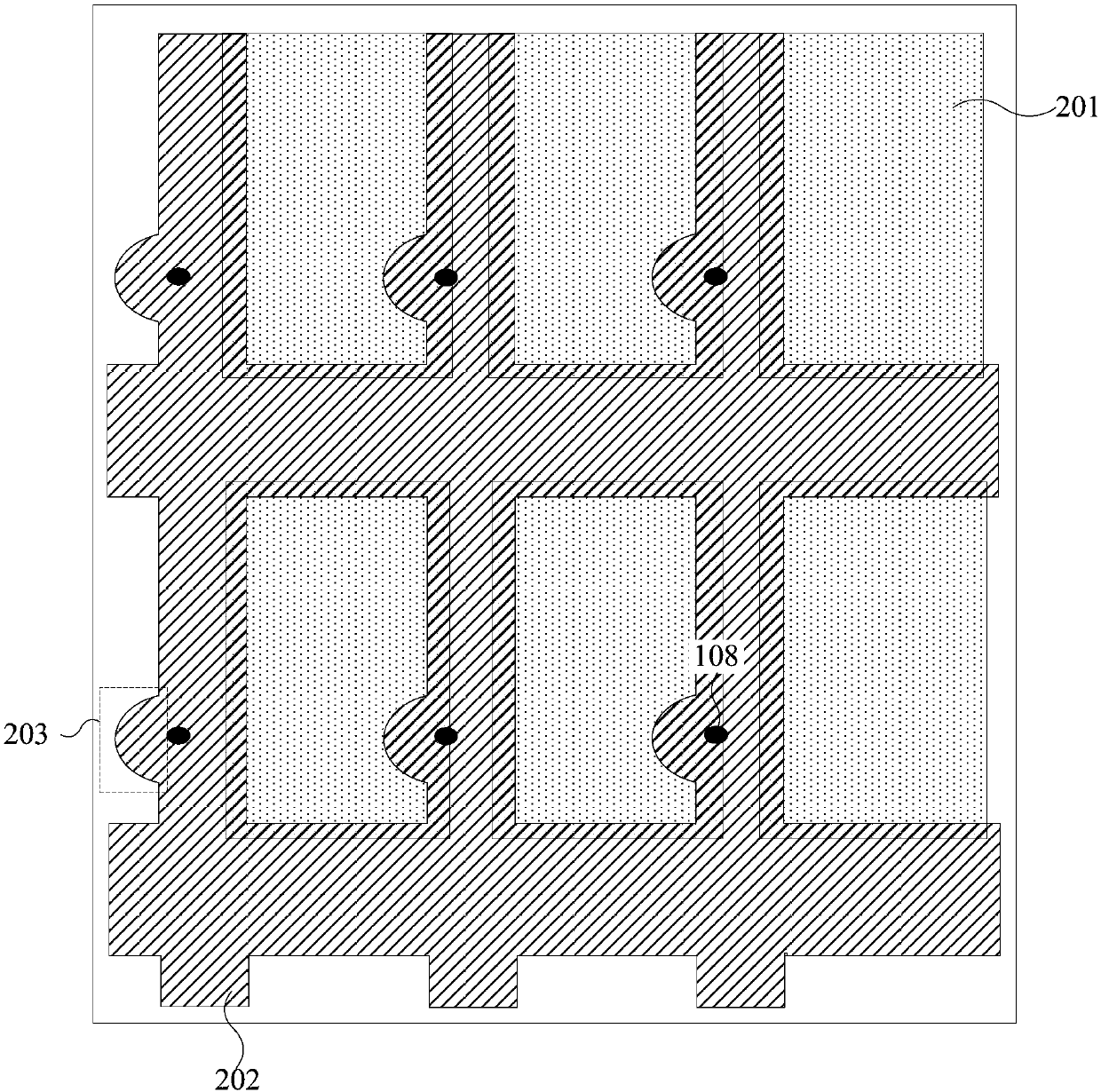
[0027] The first substrate includes a plurality of scanning lines and a plurality of data lines, the intersection of the plurality of scanning lines and the plurality of data lines defines a plurality of pixel units, each pixel unit includes a pixel electrode, the pixel electrode is electrically connected to a thin film transistor, and the thin film transistor The source electrode ...


PUM


Abstract

The invention discloses a display panel and a display device. Two adjacent pixel units in the display panel are a first pixel unit and a second pixel unit respectively. The edge, which is near a source via hole, of the first pixel unit is a first edge. The edge, which is near the source via hole, of the second pixel unit is a second edge. The minimum distance A between the edge of the source via hole and the first edge along the extending direction of a scan line is A. The minimum distance between the edge of the source via hole and the second edge is B, and A is less than B. A first color filter unit corresponds to the first pixel unit. A protruding structure is formed along at least a side, which is near the first color filter unit, of a black matrix in the extending direction of the scan line. The protruding structure is corresponding to the source via hole. According to the technical scheme provided by the embodiment of the invention, the black matrix can cover the source via hole;the phenomenon of dark-state light leakage at the position where the source via hole is located is avoided; and the display effect of the display panel is improved.

Description

technical field [0001] Embodiments of the present invention relate to display technologies, and in particular, to a display panel and a display device. Background technique [0002] With the continuous development of display technology, display devices are used in various fields of social life and are favored by users. [0003] The display panel is the core component of the display device. With the continuous improvement of the manufacturing process, the line width of each structure in the display panel is getting smaller and smaller, and the pixel density of the display panel is increasing accordingly. The source via hole and drain electrode in the pixel unit The distance between the vias becomes smaller, and the capacitive coupling between the two increases. In order to solve the above problems, the method adopted in the prior art is to move the position of the source via hole so that the source via hole is far away from the drain via hole. However, in this method, the s...

Claims


Application Information

Patent Timeline
IPC IPC(8): H01L27/12H01L29/786
Inventor 梁玉姣方丽婷郑斌义杨雁吴玲沈柏平
Owner WUHAN TIANMA MICRO ELECTRONICS CO LTD
Why Eureka
Try Eureka