Mask, encapsulation method and structure of OLED display substrate and display apparatus

A technology of a display substrate and a packaging method, which is applied to semiconductor devices, electrical components, circuits, etc., can solve the problems of large climbing distance, large distance from the edge of the display area to the obstacle, and disadvantageous narrow borders and no borders of display devices, etc. Achieve the effect of reducing the design distance and achieving a narrow frame

Active Publication Date: 2018-02-13
BOE TECH GRP CO LTD +1
View PDF3 Cites 30 Cited by
  • Summary
  • Abstract
  • Description
  • Claims
  • Application Information

AI Technical Summary

Problems solved by technology

[0002] The process steps of the existing flexible OLED packaging structure mainly include: preparing a flexible substrate→making the first gate insulating layer→making the first gate metal layer pattern→making the second gate insulating layer→making the second gate metal layer pattern→making the interlayer Insulation layer→making source-drain metal layer pattern→making flat layer→making anode→making pixel definition layer→making spacer layer→making cathode→making packaging film layer, wherein the packaging film layer includes organic and inorganic films stacked, When preparing organic thin films, rheological organic materials, such as acrylic materials, are inkjet printed in the filled area surrounded by barriers. The rheological organic materials are automatically leveled and solidified in the filled area to form an organic film. Due to the thickness of the organic film Therefore, the climbing distance of its edge is relatively large, that is, the distance from the edge of the display area to the barrier is relatively large, which is not conducive to the realization of a narrow frame and no frame of the display device.

Method used


Image

  • Mask, encapsulation method and structure of OLED display substrate and display apparatus
  • Mask, encapsulation method and structure of OLED display substrate and display apparatus
  • Mask, encapsulation method and structure of OLED display substrate and display apparatus

Examples


Embodiment Construction

[0036] In order to make the technical problems, technical solutions and advantages to be solved by the embodiments of the present invention clearer, the following will describe in detail with reference to the drawings and specific embodiments.

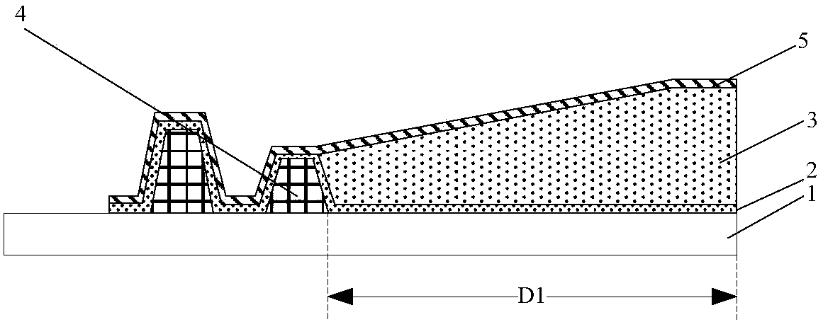
[0037] The process steps of the existing flexible OLED packaging structure mainly include: preparing a flexible substrate→making the first gate insulating layer→making the first gate metal layer pattern→making the second gate insulating layer→making the second gate metal layer pattern→making the interlayer Insulation layer→making source and drain metal layer graphics→making flat layer→making anode→making pixel definition layer→making spacer layer→making cathode→making packaging film layer, such as figure 1 As shown, wherein 1 is the base substrate of the OLED display substrate, 2 is the surface film layer of the OLED display substrate, and the encapsulation film layer covering the OLED display substrate includes an organic film 3 and an...


PUM


Abstract

The invention provides a mask, an encapsulation method and structure of an OLED display substrate and a display apparatus, which belong to the technical field of display. The mask is used for encapsulating an OLED display substrate. The OLED display substrate comprises a display area, a barrier structure arranged on the edge of the OLED display substrate and a non-display area disposed between thedisplay area and the barrier structure, the mask comprises a shading graph and a transmitting graph, and the transmitting graph corresponds to at least one part of the non-display area of the OLED display substrate. The encapsulation method comprises the following steps: printing a rheological property organic material on the OLED display substrate to enable the rheological property organic material to be formed in an area formed by encircling the barrier structure; and when the rheological property organic material is flattened, blocking the OLED display substrate by adopting the mask, and then performing the ultraviolet illumination for the OLED display substrate so as to cure the rheological property organic material disposed in the non-display area. By adopting the technical scheme ofthe invention, a narrow rim of the display apparatus can be realized.

Description

technical field [0001] The invention relates to the field of display technology, in particular to a mask plate, a packaging method and structure of an OLED display substrate, and a display device. Background technique [0002] The process steps of the existing flexible OLED packaging structure mainly include: preparing a flexible substrate→making the first gate insulating layer→making the first gate metal layer pattern→making the second gate insulating layer→making the second gate metal layer pattern→making the interlayer Insulation layer→making source-drain metal layer pattern→making flat layer→making anode→making pixel definition layer→making spacer layer→making cathode→making encapsulation film layer, wherein the encapsulation film layer includes organic film and inorganic film stacked, When preparing an organic film, the rheological organic material, such as acrylic material, is inkjet printed in the filled area surrounded by barriers. The rheological organic material is...

Claims


Application Information

Patent Timeline
Patent Type & Authority Applications(China)
IPC IPC(8): H01L51/52
CPCH10K50/80H10K50/84
Inventor 崔志明
Owner BOE TECH GRP CO LTD
Why Eureka
Try Eureka