

A crystal wafer chip dimension encapsulation line and its making method
A wafer-level chip and size packaging technology, which is applied in the direction of circuits, semiconductor/solid-state device manufacturing, electrical components, etc., can solve problems such as short circuits between metals, and achieve the effect of reducing design distance, good application prospects, and significant social and economic benefits
- Summary
- Abstract
- Description
- Claims
- Application Information
AI Technical Summary
Problems solved by technology
Method used
Image

Examples
Embodiment Construction
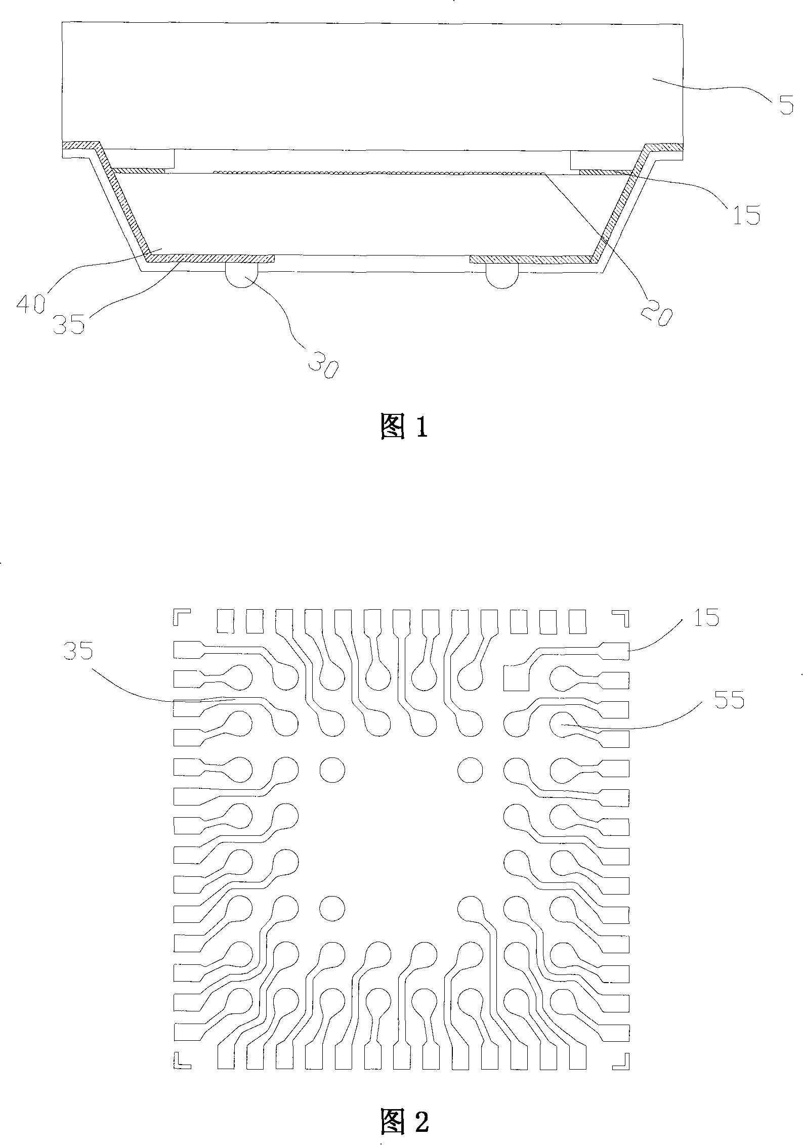
[0024] The packaging structure shown in Figure 1 is based on ShellOC technology and is a typical wafer-level chip-scale packaging. During production, firstly, the glass 5 with the cavity and the chip body 20 with the welding pad 15 are arranged and adhered, and then grinding, plasma etching, and cutting are performed sequentially to obtain a silicon inclined section or channel, and the part of the welding pad 15 is exposed. , making circuits on the bottom substrate 40, the circuits including leads and pads.
[0025] As shown in the wafer-level chip scale package circuit shown in FIG. 2 , the lead 35 is connected to the pad 15 and the pad 55 . The wires 35 connected to the pads 15 completely cover the pads 15 , and there is a certain distance between the pads 55 and the wires 35 .
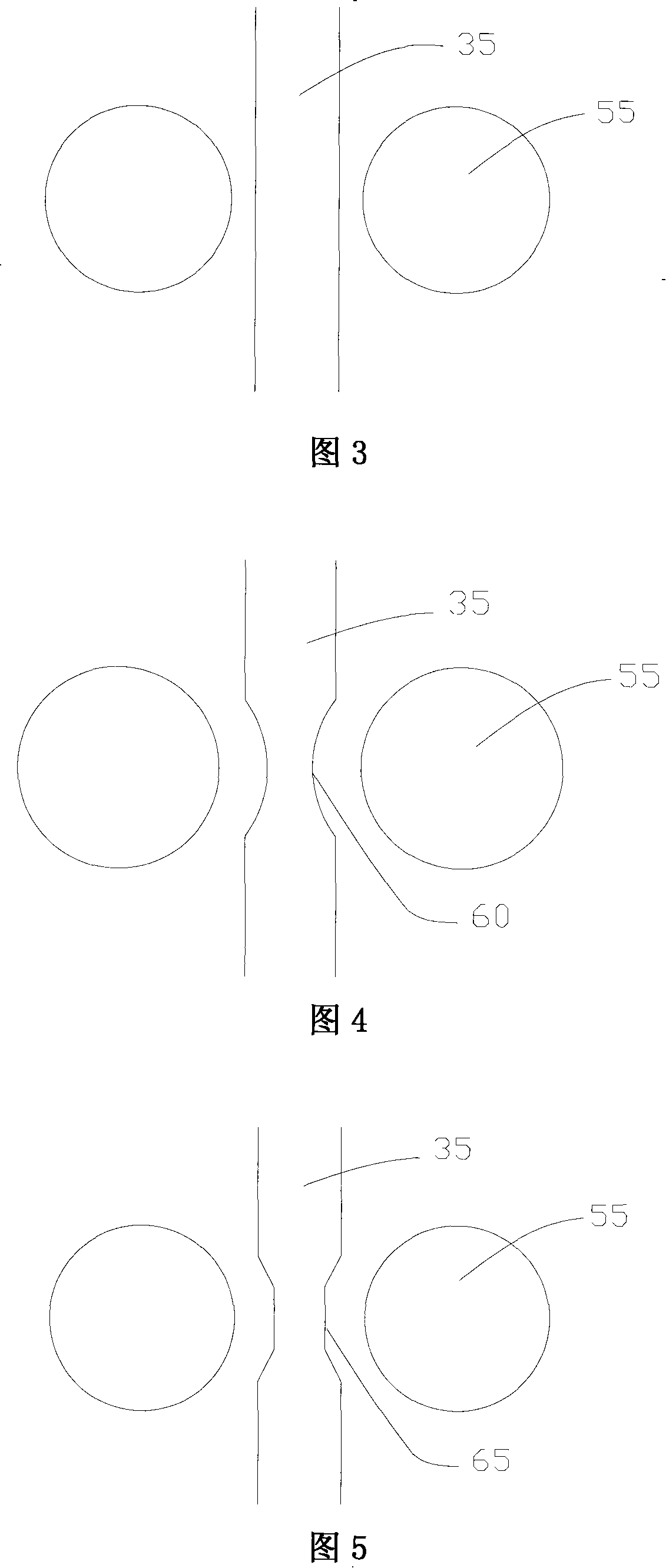
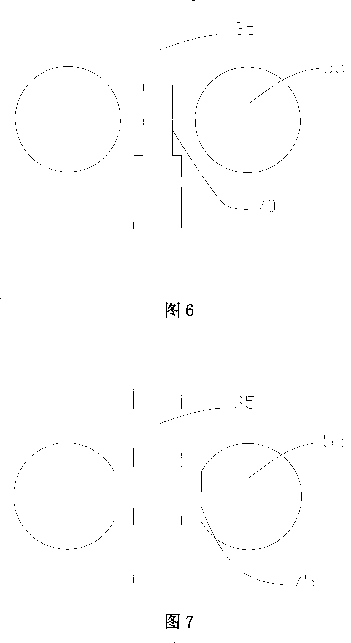
[0026] FIG. 3 is a circuit pattern of a general wafer-level chip size package, and the circuit is generally composed of leads 35 and pads 55 . In order to prevent metal-to-metal short circuit, a c...
PUM
 Abstract
Description
Claims
Application Information