GOA circuit

A circuit and low-potential technology, applied to static indicators, instruments, etc., can solve problems such as grid failure, potential pull-down, and residual image in the effective display area, so as to improve user experience and eliminate residual image.

Inactive Publication Date: 2018-03-06
WUHAN CHINA STAR OPTOELECTRONICS TECH CO LTD
View PDF5 Cites 8 Cited by
  • Summary
  • Abstract
  • Description
  • Claims
  • Application Information

AI Technical Summary

Problems solved by technology

In the case of abnormal power failure, if the NMOS-type GOA circuit cannot effectively realize the function of All GateON (that is, set all the gate driving signals in the GOA circuit to an effective potential to scan the liquid crystal display device at the same time), the panel will appear residual. film
[0004] For example, taking forward sweep as an example, in figure 1 In the GOA circuit unit shown, when an abnormal power-off is triggered, if the n+1th clock signal connected to the thin film transistor NT3 is at a high potential at this time, then the forward scanning control signal and the n+1th clock signal The potential will be pulled down to a low potential synchronously, and at the same time, the high potential of the gate of the thin film transistor NT5 cannot be released, thereby causing the thin film transistor NT5 to remain on, and at this time the thin film transistor NT8 is also in the on state, the high potential signal VGH and the low potential signal VGL Superimposed together, the gate of the thin film transistor NT7 cannot be pulled down completely, causing the thin film transistor NT7 to pull down the potential of the gate driving signal G(n) output to the thin film transistor of the pixel unit, so that the gate driving signal G(n) is not enough to turn on In the thin film transistor of the pixel unit, the charge of the pixel electrode cannot be released in time, which will cause residual image in the effective display area when the power is abnormally cut off

Method used


Image

  • GOA circuit
  • GOA circuit
  • GOA circuit

Examples


Embodiment Construction

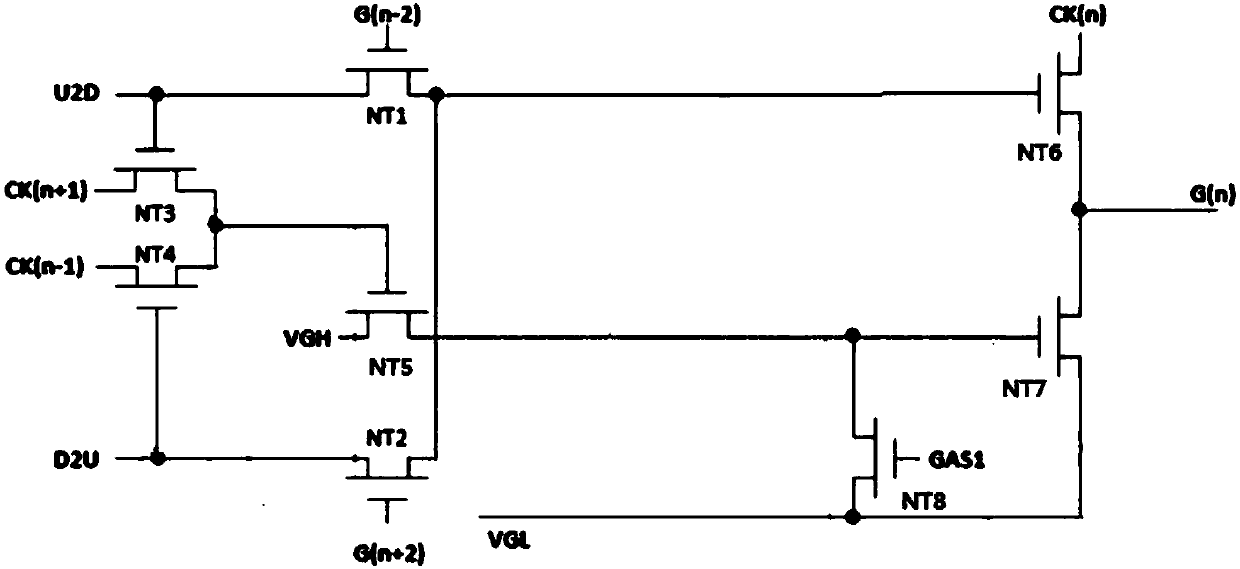
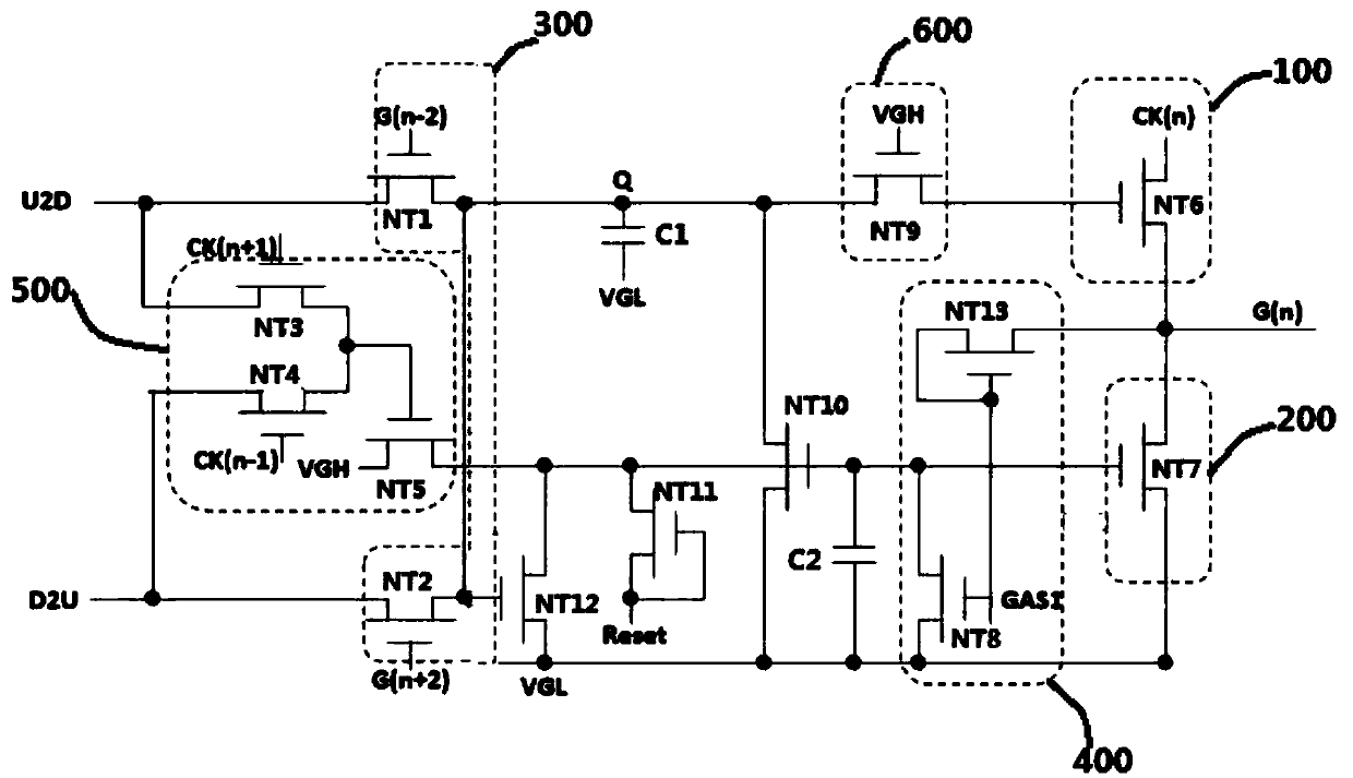
[0043] The present invention provides a GOA circuit, which is used in a liquid crystal display panel, and the GOA circuit includes m cascaded GOA units, such as figure 2 As shown, the nth level GOA unit includes: an output control module 100 , a forward and reverse scan control module 300 , a first pull-down circuit 200 , a second pull-down circuit 500 , and a pull-up circuit 400 , where m≥n≥1.

[0044] The forward and reverse scan control module 300 is used to control the GOA circuit to perform forward scan or reverse scan according to the forward scan control signal U2D or the reverse scan control signal D2U.

[0045] The output control module 100 is connected to the forward and reverse scan control module 300 , and is used to control the output of the nth-level gate drive signal G(n) during the forward scan or reverse scan period of the GOA circuit.

[0046] The first pull-down circuit 200 includes a seventh thin film transistor NT7, the first end of the seventh thin film ...


PUM


Abstract

The invention provides a GOA circuit including m cascaded GOA units. The n-th GOA unit includes: an output control module, a forward and reverse scan control module, a first pull-down circuit, a second pull-down circuit, and a pull-up circuit. The forward and reverse scan control module controls the GOA circuit to perform forward scanning or reverse scanning. The output control module controls theoutputting of the n-th gate drive signal. The first pull-down circuit includes a seventh TFT. The second pull-down circuit includes a third TFT, a fourth TFT, and a fifth TFT. The pull-up circuit includes an eighth TFT and a thirteenth TFT. After a liquid crystal display panel is powered off, the superimposed signal of the forward scan control signal and the reverse scan control signal switches off the fifth TFT and a first global control signal is a high-level signal. The GOA circuit can eliminate a residual image appearing during the abnormal power-off of the liquid crystal display panel and improves the user experience.

Description

technical field [0001] The invention relates to the field of display technology, in particular to a GOA circuit. Background technique [0002] At present, liquid crystal display devices have been widely used in various electronic products as display components of electronic equipment, and a GOA (Gate Driver On Array, GOA for short) circuit is an important part of the liquid crystal display device. The GOA circuit is a technology that uses the existing thin-film transistor liquid crystal display array manufacturing process to manufacture the gate line scanning drive signal circuit on the array substrate to realize the drive mode of progressive scanning of the gate. [0003] Display panels based on Low Temperature Polysilicon (LTPS) technology can be divided into NMOS type, PMOS type, and both NMOS and CMOS of PMOS type. Similarly, GOA circuits are divided into NMOS circuits, PMOS circuits and CMOS circuits. Compared with CMOS circuits, NMOS circuits save the PP (P doping, ...

Claims


Application Information

Patent Timeline
Patent Type & Authority Applications(China)
IPC IPC(8): G09G3/36
CPCG09G3/3677G09G2310/0286G09G2310/0283G09G2330/027G09G2320/0257
Inventor 管延庆
Owner WUHAN CHINA STAR OPTOELECTRONICS TECH CO LTD
Why Eureka
Try Eureka