Solid picture element manufacturing method

a manufacturing method and solid picture technology, applied in the field of solid picture elements, can solve the problems of residual images, inability to completely transfer charges from the bpd to the jfet, and inability to eliminate the types of potential troughs and spikes simultaneously, so as to increase the sensitivity of the solid picture element accurately, eliminate residual images securely, and improve the effect of sensitivity

Inactive Publication Date: 2007-03-06
NIKON CORP
View PDF15 Cites 7 Cited by
  • Summary
  • Abstract
  • Description
  • Claims
  • Application Information

AI Technical Summary

Benefits of technology

[0025]The solid picture element is constructed such that an edge of the charge accumulation region that is closest to the transistor is located below the transfer gate, and an edge of the depletion prevention region that is closest to the transistor is located inline or further from the transistor than the charge accumulation region and the charge accumulation region does not contact the surface of the semiconductor substrate region. By this type of structure, charges can be transferred from the charge accumulation region of the photodiode to the amplifying transistor in a solid picture element, and residual images can be substantially eliminated.
[0032]In addition, this invention provides another alternative embodiment of a method of manufacture of a solid picture element including the steps of forming a mask layer on the semiconductor substrate region, implanting ions of the second conductive type into the semiconductor substrate region using the mask layer as a mask and to form the charge accumulation region such that it is within the semiconductor substrate region and does not contact the upper surface of the semiconductor substrate region, removing the mask layer, forming the transfer gate on the semiconductor substrate region such that the position of the edge of the transfer gate on the side of the charge accumulation region is closer to the charge accumulation region than the position of the corresponding edge of the mask layer, and implanting ions of the first conductive type into the semiconductor substrate region using the transfer gate as at least part of a mask to form the depletion prevention region such that it is between the charge accumulation region and the upper surface of the semiconductor substrate region, and the edge of the charge accumulation region that faces the transistor is closer to the transistor than the edge of the depletion prevention region that faces the transistor. By this means, the charge accumulation region and the depletion prevention region can be formed to the desired profile with good control, and a solid picture element can be manufactured easily that can transfer charges completely from the charge accumulation region of the photodiode to the amplifying transistor and substantially eliminate residual images.BRIEF DESCRIPTION OF THE FIGURES

Problems solved by technology

As a result, this type of trough and spike in potential cannot be eliminated simultaneously simply by controlling the size of overlap.
Because this type of trough and spike in potential could not be completely eliminated, prior art solid picture elements have the problem that they are unable to transfer charges completely from the BPD to the JFET.
This causes residual images.
However, this is a problem because the impurity ions that form P-type charge accumulation layer 203 and N-type depletion prevention layer 204 have different diffusion coefficients.
Thus, the amount of horizontal diffusion differs for each type of ion, or is difficult to control, and it is difficult to control the size of overlap precisely.
In addition, when an overlap is formed by the difference in amount of horizontal diffusion caused by the difference in diffusion coefficients, forming an overlap of about 0.4 micrometers, for example, requires excessive heat treatment and is imprecise.
This excessive heat treatment affects other diffusion layers or causes wafer warping, and furthermore risks causing discrepancies in element characteristics.

Method used


Image

  • Solid picture element manufacturing method
  • Solid picture element manufacturing method
  • Solid picture element manufacturing method

Examples


specific embodiments

[0088]Next, the solid picture element of the present invention and its method of manufacture are explained in further detail by concrete embodiments.

first embodiment

[0089]This embodiment pertains to the method of manufacture of a solid picture element shown in FIGS. 5a-5c.

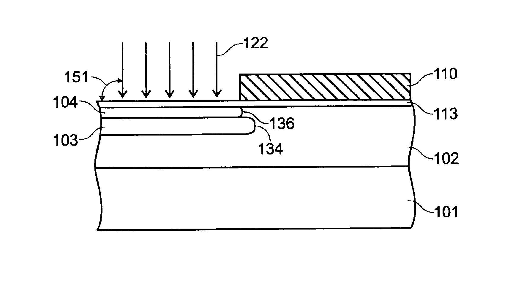
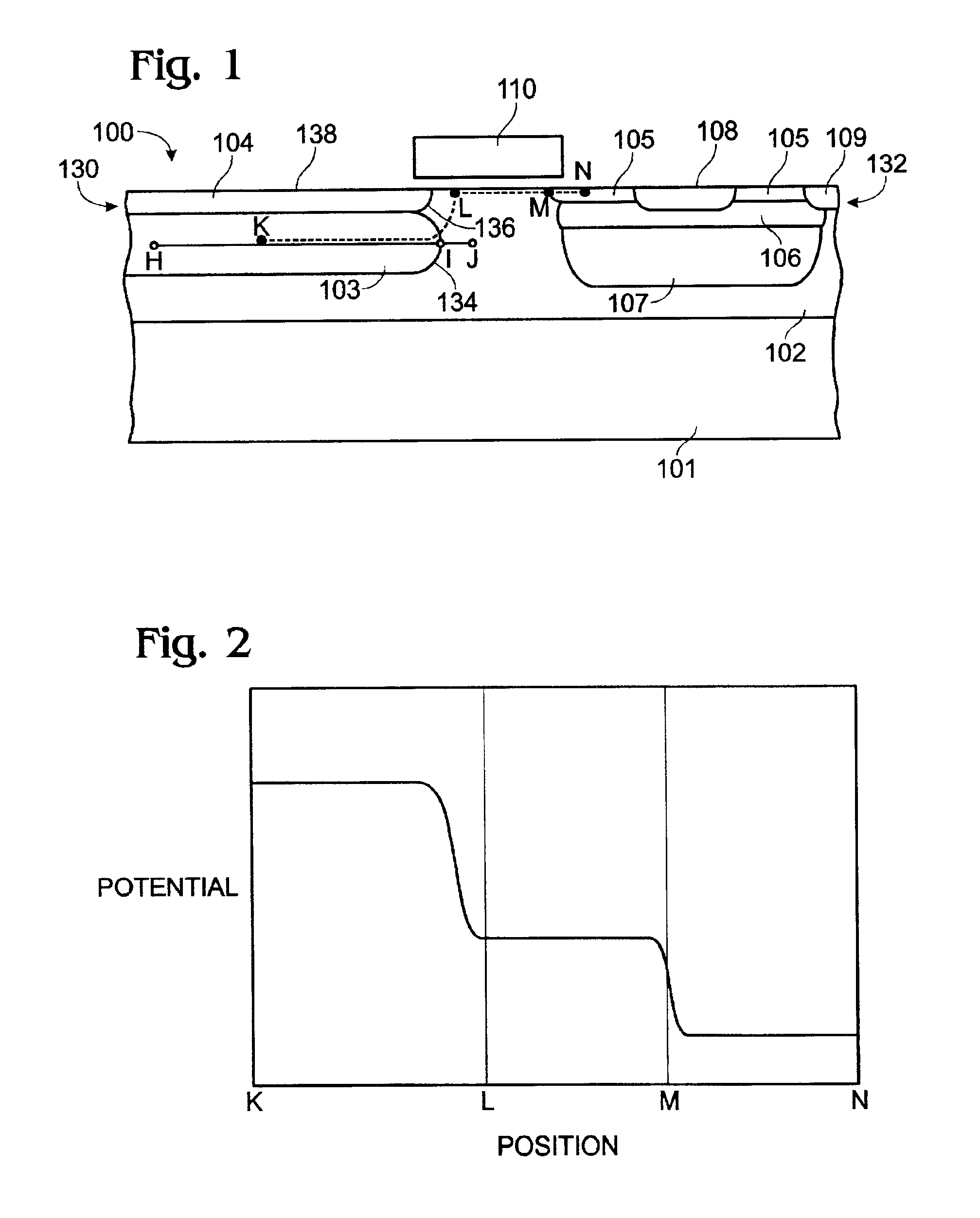
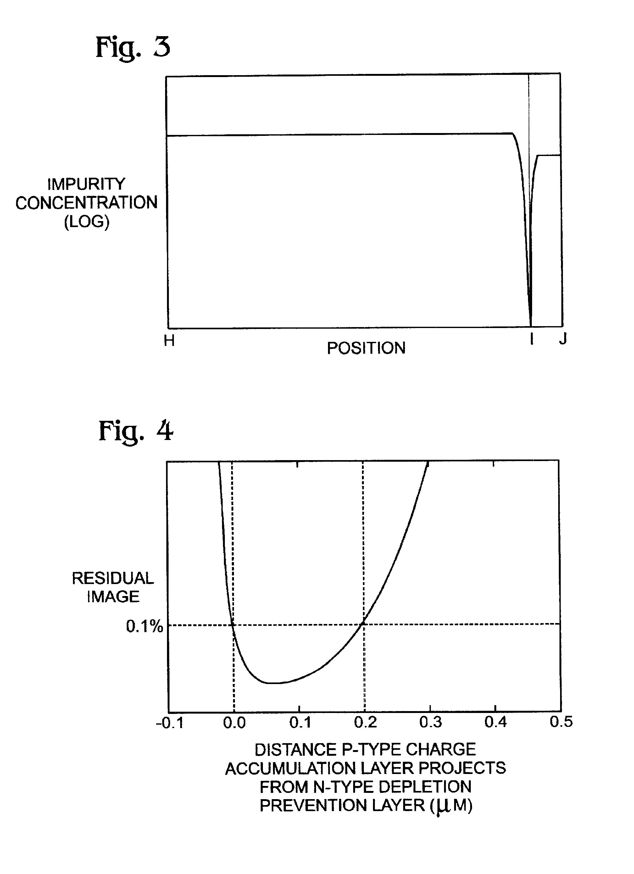
[0090]N-type well 102 was formed within P-type semiconductor substrate 101, insulating gate oxide film 113 was formed on the surface of substrate 101, and transfer gate 110 comprised of a substance such as polysilicon was formed on insulating film 113. To form P-type charge accumulation layer 103, boron was implanted by a sloping ion implantation method at a concentration of 1 to 5×1012 cm−2 and an acceleration voltage of 50 keV to 2 MeV, then heat treatment was performed in a nitrogen atmosphere at 800 to 1000° C. for approximately 30 minutes. In some cases, heat treatment may be performed by rapid thermal acceleration.

[0091]Furthermore, to form N-type depletion prevention layer 104, phosphorus was implanted at a concentration of 1 to 5×1013 cm−2 and an acceleration voltage of approximately 80 keV, then heat treatment was performed in a nitrogen atmosphere at 800 to 950° C. ...

second embodiment

[0092]This embodiment pertains to the method of manufacture of a solid picture element shown in FIGS. 6a-6c.

[0093]N-type well 102 was formed within P-type semiconductor substrate 101, insulating a gate oxide film 113 was formed on the surface of substrate 101, and transfer gate 110 comprised of a substance such as polysilicon was formed on insulating film 113. To form P-type charge accumulation layer 103, boron was implant at a concentration of 1 to 5×1012 cm−2 and an acceleration voltage of 50 keV to 2 MeV using transfer gate 110 as part of a mask, then heat treatment was performed in a nitrogen atmosphere at 800 to 1000° C. for approximately 30 minutes. In some cases, heat treatment may be performed by rapid thermal acceleration.

[0094]Following this, transfer gate 110 was oxidized by pyro-oxidation at 900 to 950° C. for 5 to 30 minutes, and an oxide film about 0.1 to 1 μm thick was formed. Furthermore, to form N-type depletion prevention layer 104, phosphorus was implanted at a c...


PUM


Abstract

A solid picture element that transfers charges completely from a photodiode portion to an amplifying transistor portion to substantially eliminate residual images and methods of its manufacture are disclosed. The solid picture element includes a buried photodiode and a transistor in communication with a transfer gate that is a selective transfer path for charges from the photodiode to the transistor. The charge accumulation region is located so that it is not in contact with the upper surface of the semiconductor substrate and so that a margin of the charge accumulation region is located 0.0 to 0.2 μm closer to the transistor than any portion of the depletion prevention region. Methods of manufacture of the picture element of the present invention include using the transfer gate as a mask and implanting ions into a semiconductor substrate at a first angle to form the charge accumulation region and at a second, steeper, angle to form the depletion prevention region. Alternative methods of manufacture include sifting a portion of a mask to sift end margins of the charge accumulation region and the depletion prevention region to achieve the desired geometry.

Description

[0001]This is a divisional of application Ser. No. 09 / 177,254, filed Oct. 22, 1998 U.S. Pat. No. 6,281,531.FIELD OF THE INVENTION[0002]This invention pertains to a solid picture element and methods of manufacture of the solid picture element. More particularly, this invention pertains to the structure of a light receiving part of the solid picture element and its methods of manufacture.BACKGROUND AND SUMMARY OF THE INVENTION[0003]A solid-state image sensing device, such as a charge-coupled device, responds to incident light to generate signal charges that are stored in a depletion region and produce an output signal at an output terminal thereof. A basic charge-coupled device includes a metal-oxide semiconductor device in which a metal electrode is positioned on, and insulated from, a silicon substrate. Charge-coupled devices, or solid picture elements, are arranged in arrays and coupled to circuitry that samples the devices for use in, for example, generating a video image.[0004]In...

Claims


Application Information

Patent Timeline
Patent Type & Authority Patents(United States)
IPC IPC(8): H01L21/339H01L21/265H01L27/146H04N5/335H04N5/357H04N5/369H04N5/374H04N5/3745
CPCH01L27/14609H01L27/14689H01L27/14643
Inventor KAMASHITA, ATSUSHISUZUKI, SATOSHI
Owner NIKON CORP
Why Eureka
Try Eureka