Display panel, production method thereof and display device

A display panel and display device technology, which is applied in the direction of identification devices, instruments, semiconductor devices, etc., can solve the problems of short-circuiting of conductive electrodes, etc., and achieve the effect of improving product yield and realizing bonded connection

Pending Publication Date: 2018-03-09
BOE TECH GRP CO LTD +1
View PDF12 Cites 15 Cited by
  • Summary
  • Abstract
  • Description
  • Claims
  • Application Information

AI Technical Summary

Problems solved by technology

[0005] Aiming at the above-mentioned deficiencies in the prior art, the present invention provides a display panel, its preparation method, and a display device, which are used to at least partially solve the problem that the conductive electrodes in the binding area of ​​the display panel are prone to short circuit

Method used


Image

  • Display panel, production method thereof and display device
  • Display panel, production method thereof and display device
  • Display panel, production method thereof and display device

Examples


Embodiment Construction

[0038] The technical solutions in the present invention will be clearly and completely described below in conjunction with the accompanying drawings in the present invention. Apparently, the described embodiments are part of the embodiments of the present invention, not all of them. Based on the embodiments of the present invention, all other embodiments obtained by persons of ordinary skill in the art without making creative efforts belong to the protection scope of the present invention.

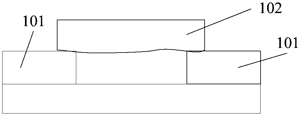
[0039] combine image 3 and Figure 5 As shown, the present invention provides a display panel 10. The display panel 10 includes a base substrate 1 and a plurality of first conductive electrodes 2 arranged on the base substrate 1. Each first conductive electrode 2 is located in the binding area, and each There is a gap d between the first conductive electrodes 2 . The display panel 10 further includes an insulating layer 4 capable of being pierced by ACF (Anisotropic Conductive Film, Ani...


PUM


Abstract

The invention provides a display panel, a production method thereof and a display device. The display panel has the advantages that an insulating layer is arranged on a first conductive electrode in adisplay panel binding area to allow the insulating layer to cover the first conductive electrode, and the insulating layer can be punctured by ACF particles; when the display panel is bound with an FPC through ACF, a second conductive electrode on the FPC can be communicated with the first conductive electrode on the display panel through the ACF particles, and accordingly binding connection of the display panel and the FPC is achieved; even if conductive foreign matter falls into the area where the first conductive electrode is located, short circuit can be avoided, and accordingly product yield is increased.

Description

technical field [0001] The invention relates to the field of display technology, in particular to a display panel, a manufacturing method thereof, and a display device. Background technique [0002] combine figure 1 , Figure 2a , Figure 2b As shown, the gap between the conductive electrodes 101 in the binding area of ​​the display panel (that is, the PAD area) is getting smaller and smaller, and the conductive electrodes 101 are metal electrodes. If the conductive foreign matter 102 falls on the conductive electrodes, it is easy to cause phase Adjacent conductive electrodes 101 are shorted. In the pixel circuit, when the voltage Vdata on the data line is high potential, the display is dark, and when Vdata is low potential, the display is bright. [0003] combine Figure 2a and Figure 2c As shown, when the screen is normally on, if the adjacent conductive electrodes 101 are short-circuited, the voltage on the conductive electrodes 101 whose input voltage is low will ...

Claims


Application Information

Patent Timeline
Patent Type & Authority Applications(China)
IPC IPC(8): G09F9/35H01L27/32
CPCG09F9/35H10K59/00H01L27/1248H01L27/1203H01L27/1237H01L27/1288H01L27/1292
Inventor 宋德雄阳智勇黄立为黄世花蒋学袁世兵陈飞李伟付超张娜杜誉邓雪梅
Owner BOE TECH GRP CO LTD
Why Eureka
Try Eureka