Voltage regulator having auto mode optimization for load profiles
A technology of voltage regulators and operating modes, which is applied in the direction of adjusting electrical variables, control/regulation systems, instruments, etc., and can solve the problems of low efficiency of switching voltage regulators, etc.
- Summary
- Abstract
- Description
- Claims
- Application Information
AI Technical Summary
Problems solved by technology
Method used
Image

Examples
Embodiment Construction
[0019] In the following description, for purposes of explanation, numerous examples and specific details are set forth in order to provide a thorough understanding of the present disclosure. However, it will be apparent to those skilled in the art that the present disclosure, as expressed in the claims, may include some or all of the features of these examples, alone or in combination with other features described below, and may also include features described herein Modifications and equivalents of and concepts.
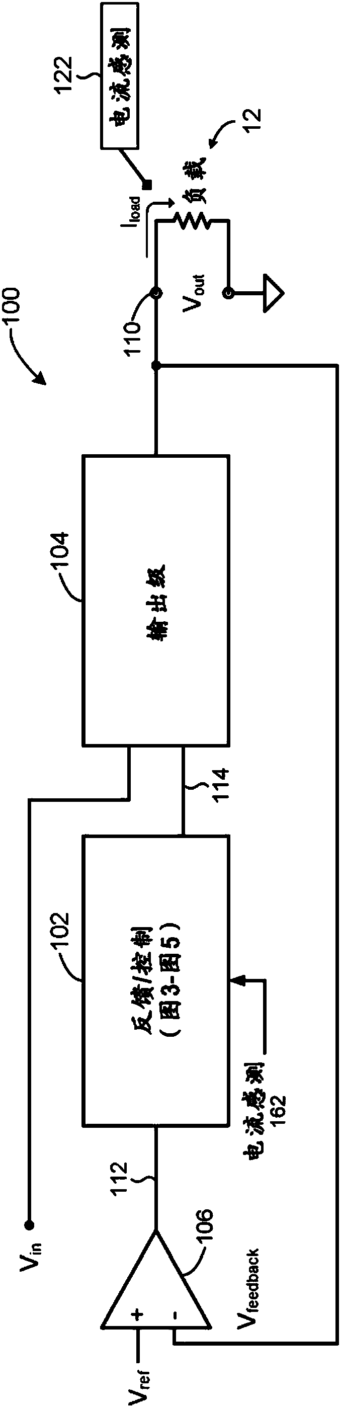
[0020] figure 1 is shown according to the present disclosure configured to generate a regulated output voltage V at the output 110 out A high-level block diagram of a voltage regulator 100 to drive a load 12 . Voltage regulator 100 may include feedback / control stage 102 and output stage 104 . Feedback signal V can be provided from output 110 feedback And through the error amplifier 106 it is compared with the reference voltage V ref A comparison is made to gen...
PUM
 Abstract
Description
Claims
Application Information
 - Generate Ideas
- Intellectual Property
- Life Sciences
- Materials
- Tech Scout
- Unparalleled Data Quality
- Higher Quality Content
- 60% Fewer Hallucinations
Browse by: Latest US Patents, China's latest patents, Technical Efficacy Thesaurus, Application Domain, Technology Topic, Popular Technical Reports.
© 2025 PatSnap. All rights reserved.Legal|Privacy policy|Modern Slavery Act Transparency Statement|Sitemap|About US| Contact US: help@patsnap.com