Interface bus for utility-grade network communication devices

a network communication device and interface bus technology, applied in the field of intelligent communications devices, can solve the problems of inability to monitor and control the operability of electronic devices and modules connected to the main circuit board, the inability to anticipate, detect and respond to system problems by using standard hardware interfaces, and the inability to change the whole apparatus

Active Publication Date: 2014-11-04
ITRON
View PDF64 Cites 139 Cited by
  • Summary
  • Abstract
  • Description
  • Claims
  • Application Information

AI Technical Summary

Benefits of technology

[0009]In one embodiment, the intelligent communications device has a programmable processor that is operative to cause a device to receive relevant device monitoring data on secondary circuit boards and on field replaceable units (FRUs) that are connected to a main circuit board, from sensors, using standard hardware interfaces. The programmable processor is operative to control, monitor and respond to various functional needs of the overall system. A management information database (MIB) keeps a log of internal events. SNMP tools can access the MIB where predetermined parameters are available, and the programmable processor can cause the system to respond to changes in operability conditions, according to predetermined parameters. The programmable processor is further operable to cause the selective enabling or disabling of secondary circuit boards on the main circuit board through a hardware interface bus, in response to any detected changes in predetermined parameters.

Problems solved by technology

When it is not possible to replace the individual electronic devices mounted on the main circuit board, the whole apparatus may need to be changed.
Also, it may not be feasible to monitor and control the operability of the electronic devices and modules connected to the main circuit board when extreme environmental conditions exist.
Conventional methods of configuring electronic devices of a main circuit board do not provide for an option to anticipate, detect and respond to system problems by using standard hardware interfaces.

Method used


Image

  • Interface bus for utility-grade network communication devices
  • Interface bus for utility-grade network communication devices
  • Interface bus for utility-grade network communication devices

Examples


Embodiment Construction

[0019]Description of the various embodiments detailed below is for understanding the invention. It will be understood that the invention is not limited to the particular embodiments described herein, but is capable of various modifications, rearrangements and substitutions, which will now become apparent to those skilled in the art without departing from the scope of the invention. Therefore, it is intended that the following claims cover all such modifications and changes that fall within the spirit and scope of the invention.

[0020]In alternative embodiments, system, process, and apparatus may include additional, fewer, or different components. In addition, the each component may include additional modules, software, and interface devices that may be appended on requirement to operate the present invention in alternate embodiments.

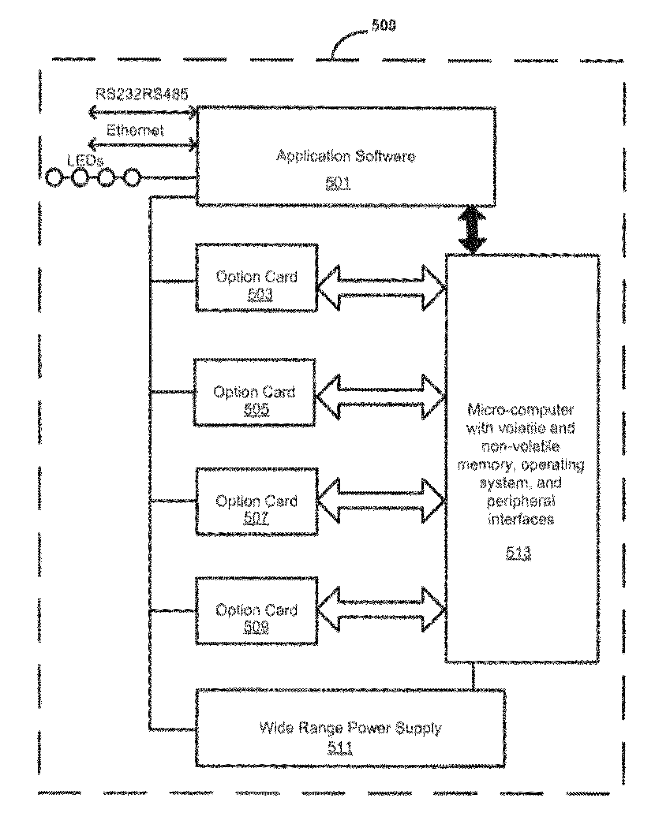
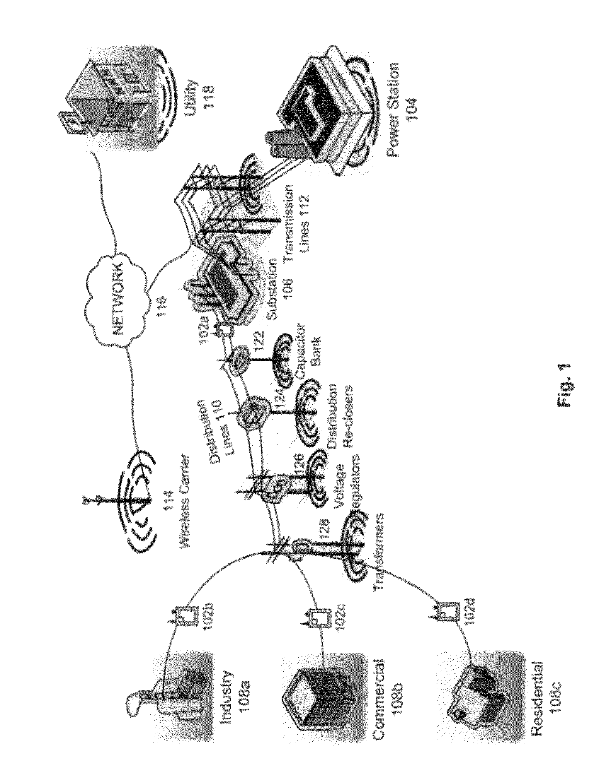
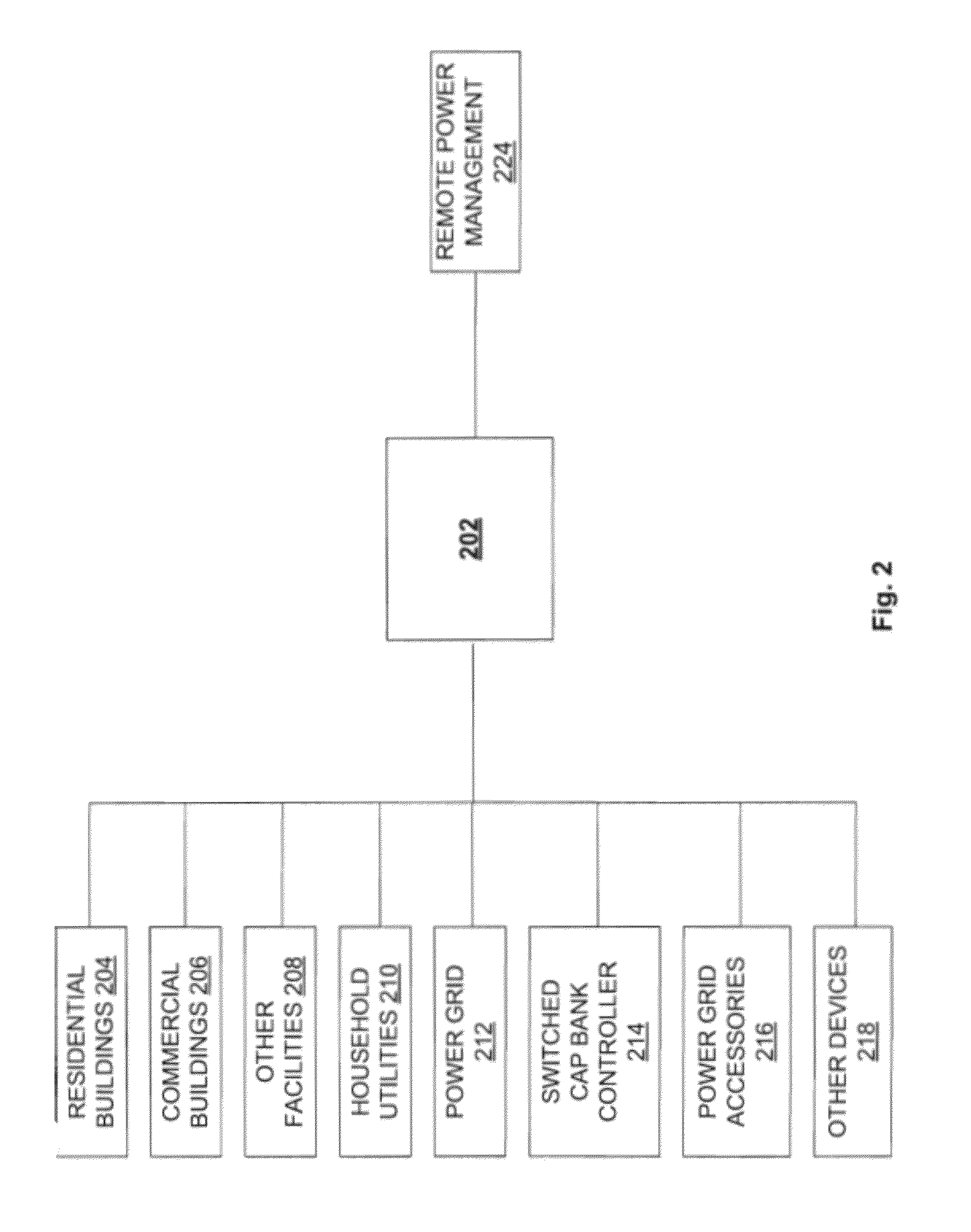
[0021]Referring to FIG. 1, an intelligent communications device for a smart grid communicatively coupled to a plurality of devices and / or facilities for ...


PUM


Abstract

In one embodiment, a network device having a plurality of hardware interfaces is disclosed. The network device includes a central processing unit and a main circuit board. The main circuit board has expansion slots that receivably connect corresponding secondary circuit boards to the main circuit board. The main circuit board also has sensors for detecting predetermined parameters. A voltage regulator is operative to regulate one or more particular expansion slots, in response to detection of a predetermined parameter associated with respective slots.

Description

CROSS REFERENCE TO RELATED PATENT APPLICATION[0001]This application claims the benefit, pursuant to 35 U.S.C. §119(e) of U.S. provisional Application Ser. No. 61 / 377,025, filed Aug. 25, 2010, entitled “Interface Bus for Utility-Grade Network Communication Devices” by Charles W. Melvin, Robert B. Seal, Phillip Warren, and Edward G. Howard, the disclosure for which is hereby incorporated by reference in its entirety.FIELD OF THE INVENTION[0002]The present application relates generally to network routers, and more specifically to an intelligent communications device for a smart grid, hereinafter also referred to as an “apparatus” or “network apparatus”, for managing interconnection of various electrical devices and facilities.[0003]In one aspect, the present invention relates to monitoring and control of field replaceable units, and in particular monitoring and controlling operability of secondary circuit boards mounted that are operatively connected to the main circuit board.BACKGROUN...

Claims


Application Information

Patent Timeline
Patent Type & Authority Patents(United States)
IPC IPC(8): G06F13/14
CPCY02E60/7853H02J13/0075H02J13/0079Y04S40/126H02J13/00024H02J13/00026H02J13/00028H02J13/00034Y02E60/00
Inventor MELVIN, JR., CHARLES W.SEAL, ROBERT BRYANWARREN, PHILLIPHOWARD, EDWARD GLENN
Owner ITRON
Why Eureka
Try Eureka