A kind of oled device and manufacturing method thereof

A manufacturing method and device technology, which are applied in semiconductor/solid-state device manufacturing, semiconductor devices, electric solid-state devices, etc., can solve the problems of increasing the cost of organic light-emitting diodes, increasing the process time, reducing the success rate of organic light-emitting diodes, etc. Fabrication efficiency, enhanced microcavity effect, time and cost saving effect

Active Publication Date: 2019-06-25
WUHAN CHINA STAR OPTOELECTRONICS SEMICON DISPLAY TECH CO LTD
View PDF2 Cites 0 Cited by
  • Summary
  • Abstract
  • Description
  • Claims
  • Application Information

AI Technical Summary

Problems solved by technology

This not only increases the time of the process, but also greatly increases the cost of the organic light-emitting diode due to the problem of metal mask cleaning.
Moreover, it will also cause alignment issues in the use of fine metal masks, which greatly reduces the success rate of organic light-emitting diodes.

Method used


Image

  • A kind of oled device and manufacturing method thereof
  • A kind of oled device and manufacturing method thereof
  • A kind of oled device and manufacturing method thereof

Examples


Embodiment 1

[0055] Corresponding to Embodiment 1 of the present invention, Embodiment 2 of the present invention provides an OLED device, such as Figure 4 shown, including:

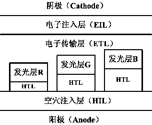
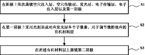
[0056] an anode, and a hole injection layer, a hole transport layer, a light-emitting layer, an electron transport layer, an electron injection layer and a first cathode formed by sequential vapor deposition on the anode;

[0057] Forming an organic material layer corresponding to each sub-pixel of the light-emitting layer and used to adjust the microcavity effect on the first cathode by photolithography;

[0058] A second cathode formed by vapor deposition on the organic material layer.

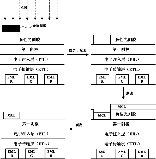
[0059] Wherein, the organic material layer is formed in the following manner:

[0060] A photomask is set at the position corresponding to the sub-pixel of the light-emitting layer, and the negative photoresist is exposed and developed by using the photomask;

[0061] Evaporating a layer of organic material layer for adjusting ...


PUM


Abstract

The present invention provides an OLED device and a manufacturing method thereof, wherein the manufacturing method includes: step S1, sequentially evaporating a hole injection layer, a hole transport layer, a light-emitting layer, an electron transport layer, an electron injection layer, and a first Cathode; step S2, forming an organic material layer corresponding to each sub-pixel of the light-emitting layer on the first cathode by photolithography for adjusting the microcavity effect; step S3, evaporating a second cathode on the organic material layer. In the present invention, a photolithography process that has no effect on the OLED material is added between the two layers of cathodes to add a conductive organic material layer, and the microcavity effect is enhanced by adjusting the film thickness of the layer. The photolithography process is different from the photolithography process for making CF and anode. , does not require a fine metal mask, thereby saving the time and cost of the OLED manufacturing process and increasing the production efficiency.

Description

technical field [0001] The invention relates to the technical field of screen display, in particular to an OLED device and a manufacturing method thereof. Background technique [0002] Organic light-emitting diode OLED (Organic light-emitting Diode) self-luminous display through the organic layer, because it does not require a backlight source, it has faster response time, larger viewing angle, higher contrast ratio and lighter component quality , low power consumption and other characteristics, it is currently recognized as the most potential flat panel display technology. [0003] Organic light-emitting diodes consist of multilayer structures with different functions. The intrinsic properties of each layer material and its compatibility with other layer materials are very important. In a multilayer structure, a hole injection layer (HIL), a hole transport layer (HTL), an emission layer (EML), an electron transport layer (ETL), and an electron injection layer (EIL) are us...

Claims


Application Information

Patent Timeline
Patent Type & Authority Patents(China)
IPC IPC(8): H01L51/56H01L51/52
CPCH10K50/85H10K71/00
Inventor 任泓扬徐湘伦
Owner WUHAN CHINA STAR OPTOELECTRONICS SEMICON DISPLAY TECH CO LTD
Why Eureka
Try Eureka