Display panel and display device

A technology for display panels and display devices, which can be applied to semiconductor devices, electrical components, circuits, etc., and can solve the problems of poor display uniformity of display panels.

Active Publication Date: 2018-04-06
WUHAN TIANMA MICRO ELECTRONICS CO LTD
View PDF7 Cites 32 Cited by
  • Summary
  • Abstract
  • Description
  • Claims
  • Application Information

AI Technical Summary

Problems solved by technology

[0005] Embodiments of the present invention provide a display panel and a display device, which are used to solve the problem in the pr

Method used


Image

  • Display panel and display device
  • Display panel and display device
  • Display panel and display device

Examples


Embodiment Construction

[0044] Aiming at the problem in the prior art that the display uniformity of the display panel is poor due to the severe voltage drop on the power supply voltage signal line, the embodiments of the present invention provide a display panel and a display device.

[0045] The specific implementation manners of the display panel and the display device provided by the embodiments of the present invention will be described in detail below with reference to the accompanying drawings. The size and shape of each structure in the drawings do not reflect the real scale, but are only intended to schematically illustrate the content of the present invention.

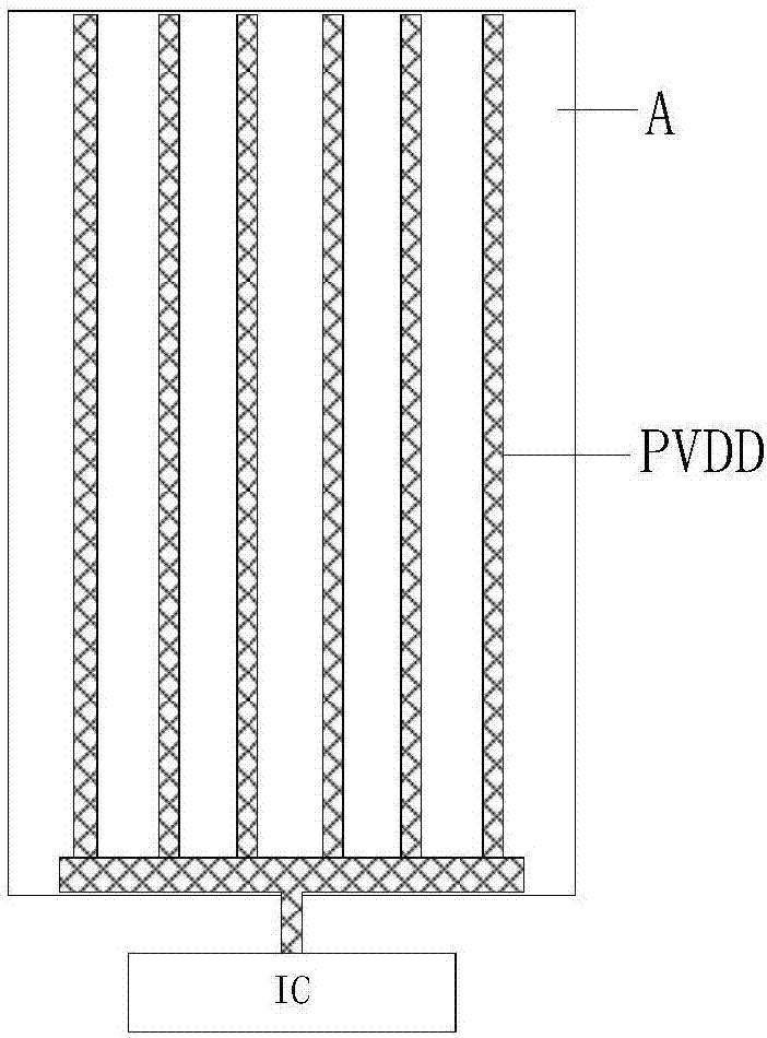
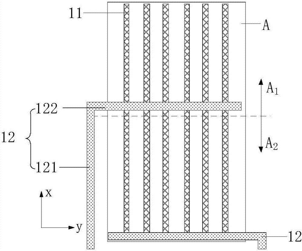
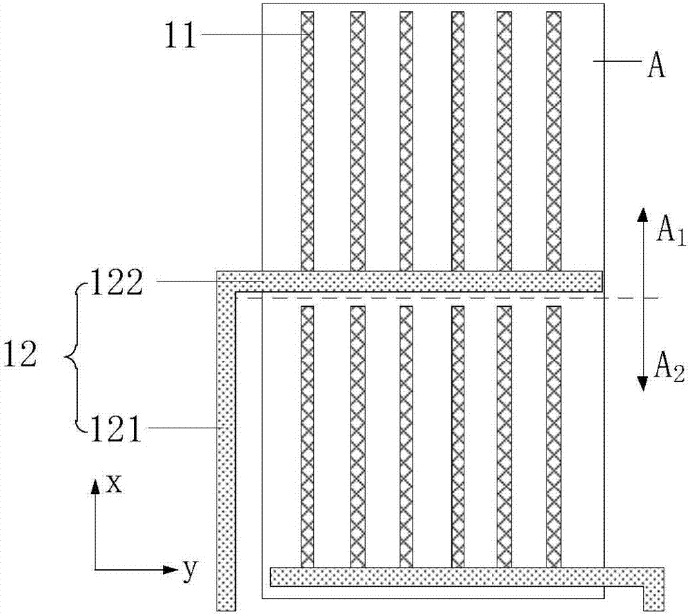
[0046] In a first aspect, an embodiment of the present invention provides a display panel, such as figure 2 shown, including the display area (such as figure 2 In the area A) and the non-display area (not shown in the figure), in the first direction of the display panel (such as figure 2 The direction indicated by the arrow x i...


PUM


Abstract

The invention discloses a display panel and a display device. The display panel comprises a display area and a non-display area. The display area comprises at least two sub-display areas in the firstdirection of the display panel. The display panel also comprises multiple power voltage signal lines extending along the first direction and signal wiring lines which are arranged in different layersfrom the power voltage signal lines. Each signal wiring line is electrically connected with each power voltage signal line in each sub-display area. The linewidth of the signal wiring lines is greaterthan that of the power voltage signal lines. According to the display panel, the power voltage is inputted to the power voltage signal lines through the area division mode so that the voltage drop onthe power voltage signal lines can be reduced. Besides, the linewidth of the signal wiring lines is greater than that of the power voltage signal lines so that the voltage drop on the power voltage signal lines can be further reduced and the display homogeneity of the display panel can be enhanced.

Description

technical field [0001] The invention relates to the field of display technology, in particular to a display panel and a display device. Background technique [0002] In the field of display, Organic Light-Emitting Diode (OLED) has the advantages of self-luminescence, fast response, wide viewing angle, high brightness, bright color, light and thin, etc., and is considered to be the next generation display technology. [0003] In OLED display panels, refer to figure 1 , the driver chip (IC) supplies the display area (i.e. figure 1 Each pixel in the region A) in , provides power to drive the light emitting diode in each pixel to emit light, for a clearer illustration. However, since each power supply voltage signal line is connected to a column of pixels, and because the OLED display panel is driven by current, each pixel has a certain resistance, so a certain voltage drop (IR-Drop) will occur every time the power supply voltage signal line passes through a pixel. ), so, in ...

Claims


Application Information

Patent Timeline
IPC IPC(8): H01L27/32
CPCH10K59/131
Inventor 马扬昭
Owner WUHAN TIANMA MICRO ELECTRONICS CO LTD
Why Eureka
Try Eureka