
Image reader device, and semiconductor device
An image reading device and image reading technology, which are applied to image communication, TV, color TV parts, etc., can solve problems such as defects in the read image, achieve the effect of correcting offset and improving the quality of reading
- Summary
- Abstract
- Description
- Claims
- Application Information
AI Technical Summary
Problems solved by technology
Method used
Image

Examples
no. 2 approach
[0193]Hereinafter, with regard to the multifunction peripheral 1 (multifunction device) to which the image reading device of the second embodiment is applied, the same reference numerals are given to the same components as those in the first embodiment, and overlapping descriptions with the first embodiment will be omitted. Differences from the first embodiment will be described.
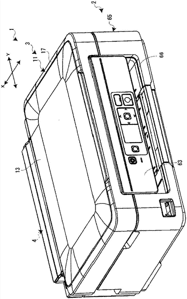
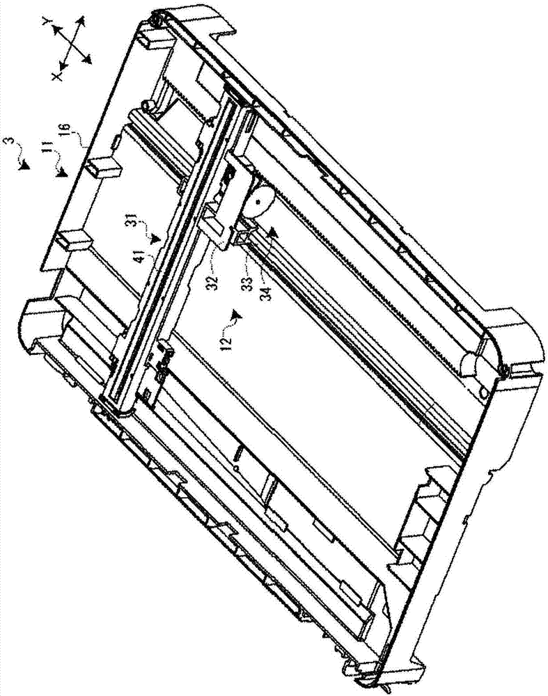
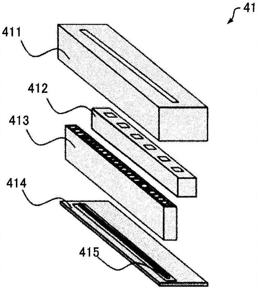
[0194] Since the structure of the multifunction peripheral 1 to which the image reading device of the second embodiment is applied is different from that of the first embodiment ( Figure 1 to Figure 4 ) are the same, so their illustrations and descriptions are omitted. Furthermore, since the functional configuration diagram of the scanner unit 3 of the second embodiment ( Figure 5 ) is the same as the first embodiment, so its illustration and description are omitted. In addition, since the functional configuration diagram of the image reading chip 415 of the second embodiment ( Image 6 ) is th...
PUM
 Abstract
Description
Claims
Application Information