Photoelectric sensing device and electronic equipment

A photoelectric sensing and photosensitive pixel technology, applied in the field of photoelectric sensing, can solve problems such as inability to obtain clear images, and achieve the effects of reducing thickness, reducing cost, and improving sensing accuracy

Active Publication Date: 2018-04-24
柳州梓博科技有限公司
View PDF15 Cites 3 Cited by
  • Summary
  • Abstract
  • Description
  • Claims
  • Application Information

AI Technical Summary

Problems solved by technology

[0003] However, the above-mentioned optical fingerprint identificati

Method used


Image

  • Photoelectric sensing device and electronic equipment
  • Photoelectric sensing device and electronic equipment
  • Photoelectric sensing device and electronic equipment

Examples


Example Embodiment

[0039] The embodiments of the present invention are described in detail below. Examples of the embodiments are shown in the accompanying drawings, wherein the same or similar reference numerals indicate the same or similar elements or elements with the same or similar functions. The following embodiments described with reference to the accompanying drawings are exemplary, and are only used to explain the present invention, but should not be understood as limiting the present invention.

[0040] In the description of the present invention, it should be understood that the terms "first" and "second" are only used for description purposes, and cannot be understood as indicating or implying relative importance or implicitly indicating the number of indicated technical features. Therefore, the features defined with "first" and "second" may explicitly or implicitly include one or more of the features. In the description of the present invention, "plurality" means two or more than two, ...


PUM


Abstract

The invention discloses a photoelectric sensing device and electronic equipment. The photoelectric sensing device comprises a semiconductor substrate, wherein the semiconductor substrate comprises a first surface and a second surface opposite to the first surface; a plurality of light sensitive pixels are formed on the first surface of the semiconductor substrate; a plurality of through holes which pass through the semiconductor substrate toward the first surface are formed on the second surface of the semiconductor substrate; and the through holes correspond to the light sensitive pixels. Theelectronic equipment comprises the photoelectric sensing device.

Description

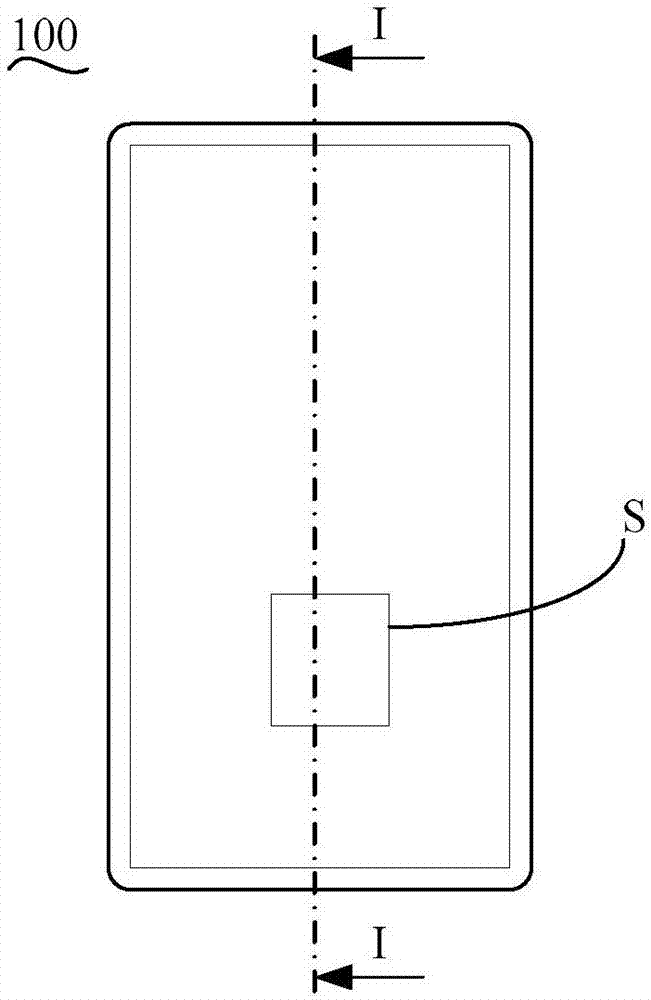
technical field [0001] The invention relates to the field of photoelectric sensing, in particular to a photoelectric sensing device and electronic equipment. Background technique [0002] At present, biometric information sensors, especially fingerprint recognition sensors, have gradually become standard components of electronic products such as mobile terminals. Since the optical fingerprint recognition sensor has a stronger penetration capability than the capacitive fingerprint recognition sensor, an optical fingerprint recognition module applied to a mobile terminal has been proposed. Such as figure 1 As shown, the optical fingerprint identification module includes an optical fingerprint sensor 400 and a light source 402 . Wherein, the optical fingerprint sensor 400 is disposed under the protective cover 401 of the mobile terminal. The light source 402 is disposed adjacent to one side of the optical fingerprint identification sensor 400 . When the user's finger F touc...

Claims


Application Information

Patent Timeline
IPC IPC(8): G06K9/00H04M1/02G06F1/16
CPCH04M1/026G06F1/1684G06V40/1324G06V40/1318
Inventor 李问杰
Owner 柳州梓博科技有限公司
Why Eureka
Try Eureka