

LED panel display structure
A display and panel technology, applied in the direction of static indicators, instruments, electric solid devices, etc., can solve the problems of inability to install driver ICs, inability to achieve small-area high-resolution, etc., and achieve the effect of reducing manufacturing costs
- Summary
- Abstract
- Description
- Claims
- Application Information
AI Technical Summary
Problems solved by technology
Method used
Image

Examples
Embodiment Construction
[0017] The above-mentioned purpose of the present invention and its structural and functional characteristics will be described according to the preferred embodiments of the accompanying drawings.
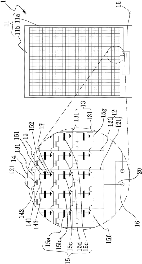
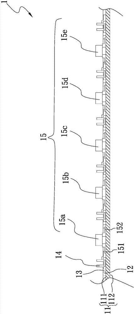
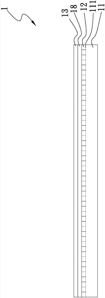
[0018] Such as figure 1 , figure 2 As shown, they are respectively the top view and combined cross-sectional view of the first embodiment of the LED panel display structure provided by the present invention. As shown in the figure, the LED panel display structure 1 provided by the present invention includes: a base 11, a first electrode layer 12. A second electrode layer 13, a plurality of switching elements 14, a plurality of light emitting diode elements 15 and a control chip 16;
[0019] The base 11 has a first side 111 and a second side 112 , and the base 11 is any one of glass, film or flexible substrate.
[0020] The first electrode layer 12 has a plurality of first electrode lines 121, and the plurality of first electrode lines 121 are longitudinally extended and arranged...
PUM
 Abstract
Description
Claims
Application Information