Multi-chip framework package structure and manufacturing method thereof

A packaging structure and multi-chip technology, which is applied in semiconductor/solid-state device manufacturing, electrical components, electric solid-state devices, etc., can solve the problems of limiting feasibility and restricting packaging density, so as to solve the limited number of chips and increase the number , the effect of meeting the diverse needs of packaging

Active Publication Date: 2018-04-24
SANECHIPS TECH CO LTD
View PDF4 Cites 0 Cited by
  • Summary
  • Abstract
  • Description
  • Claims
  • Application Information

AI Technical Summary

Problems solved by technology

[0003] QFP (Quad Flat Package) is a surface-mount package. The connection between the internal chip and the board level is completed by leading out pins of different shapes on the four sides. Because the size of the carrier table used to place the chip in the QFP middle frame is related to the size of the chip The number of pins is closely related, so it limits the feasib

Method used


Image

  • Multi-chip framework package structure and manufacturing method thereof
  • Multi-chip framework package structure and manufacturing method thereof
  • Multi-chip framework package structure and manufacturing method thereof

Examples


Embodiment 1

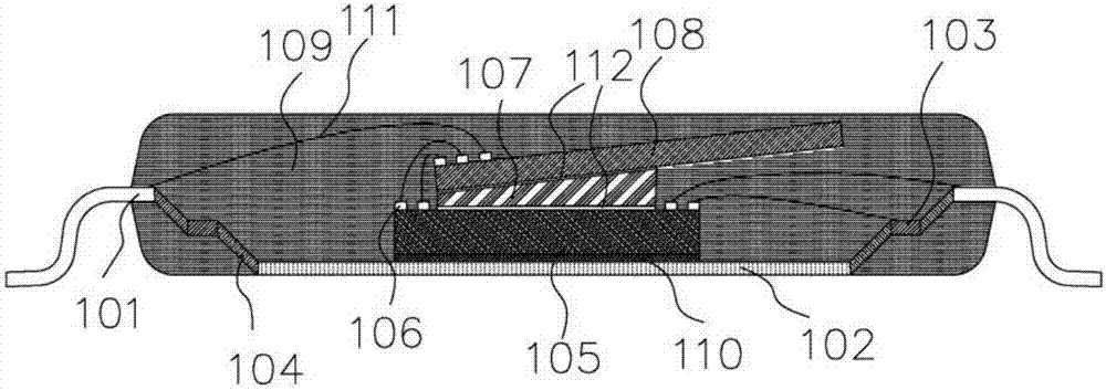
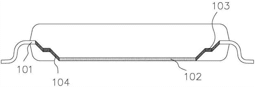
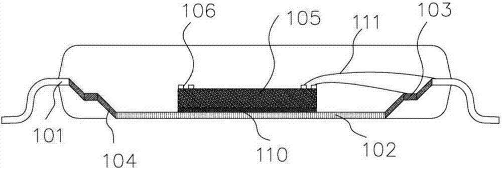
[0038] This embodiment provides a multi-chip frame packaging structure; the multi-chip frame packaging structure described in this embodiment can effectively increase the number of chips packaged in a frame SIP package, which meets the needs of packaging diversification, and effectively solves the existing SiP frame packaging structure for the problem of the limited number of chips in multi-chip packaging; specifically, the multi-chip frame packaging structure includes: at least one chip carrier, at least one bottom chip and at least one upper chip; the at least one carrier The chip platform is used to accommodate the at least one bottom chip and the at least one upper chip; the packaging structure also includes: at least one first dielectric layer; wherein, the first dielectric layer is placed above the bottom chip The upper chip is placed above the first dielectric layer; the positional relationship between the bottom chip and the upper chip can be adjusted by adjusting the i...

Embodiment 2

[0059] This embodiment provides a method for manufacturing the multi-chip frame package structure described in Embodiment 1; specifically, the method includes:

[0060] The bottom chip is set on the at least one loading stage; the first dielectric layer is set on the bottom chip, and the first dielectric layer is placed above the bottom chip; The upper chip is arranged above the dielectric layer, and the above upper chip is placed above the first dielectric layer; wherein, the bottom chip and the upper chip can be adjusted by adjusting the inclination angle of the first dielectric layer The positional relationship among them, so as to increase the number of chips stacked on the at least one loading stage.

[0061] In a specific embodiment, the packaging structure further includes: at least one second dielectric layer; correspondingly, the method further includes: disposing the second dielectric layer above the first upper layer chip in the at least one upper layer chip A diel...


PUM


Abstract

One embodiment of the invention provides a multi-chip framework package structure which includes at least one carrier table, at least one bottom chip and at least one upper chip. The at least one carrier table is used for accommodating the at least one bottom chip and the at least one upper chip. The package structure further includes at least one first medium layer which is disposed above the atleast one bottom chip. The at least one upper chip is disposed above the at least one first medium layer. The position relationship between the at least one bottom chip and the at least one upper chipcan be adjusted by adjusting the tilt angle of the at least one first medium layer, so that the number of chips stacked on the at least one carrier table can be increased. The other embodiment of theinvention provides a manufacturing method of the multi-chip framework package structure.

Description

technical field [0001] The invention relates to semiconductor device packaging technology, in particular to a multi-chip frame packaging structure and a manufacturing method thereof. Background technique [0002] Today, with the gradual development of electronic engineering, miniaturized, lightweight and functional integrated circuit (IC) chips are becoming more and more popular. Moreover, as the semiconductor industry's crystal garden process is about to reach the bottleneck, packaging technology will become an important role in improving chip manufacturing profits and challenging Moore's Law. Under this huge demand, semiconductor packaging density will continue to increase. From the development of one component, it has gradually entered the stage of integrating multiple components into a system. As a multi-chip packaging technology, system-in-package (SiP) is the current and future development trend of packaging technology. Its packaging forms are diverse, and according ...

Claims


Application Information

Patent Timeline
IPC IPC(8): H01L25/065H01L23/16H01L21/50
CPCH01L25/0657H01L21/50H01L23/16H01L2924/181H01L25/065H01L2224/32145H01L2224/48091H01L2224/48145H01L2224/48247H01L2924/00012H01L2924/00014
Inventor 谢业磊
Owner SANECHIPS TECH CO LTD
Why Eureka
Try Eureka