Method and apparatus of moving focus ring for plasma etcher

A plasma and focus ring technology, used in semiconductor/solid-state device manufacturing, discharge tubes, electrical components, etc.

Inactive Publication Date: 2018-06-05
TAIWAN SEMICON MFG CO LTD
View PDF0 Cites 0 Cited by
  • Summary
  • Abstract
  • Description
  • Claims
  • Application Information

AI Technical Summary

Problems solved by technology

However, with the reduction of the minimum wire diameter, additiona

Method used


Image

  • Method and apparatus of moving focus ring for plasma etcher
  • Method and apparatus of moving focus ring for plasma etcher
  • Method and apparatus of moving focus ring for plasma etcher

Examples


Embodiment Construction

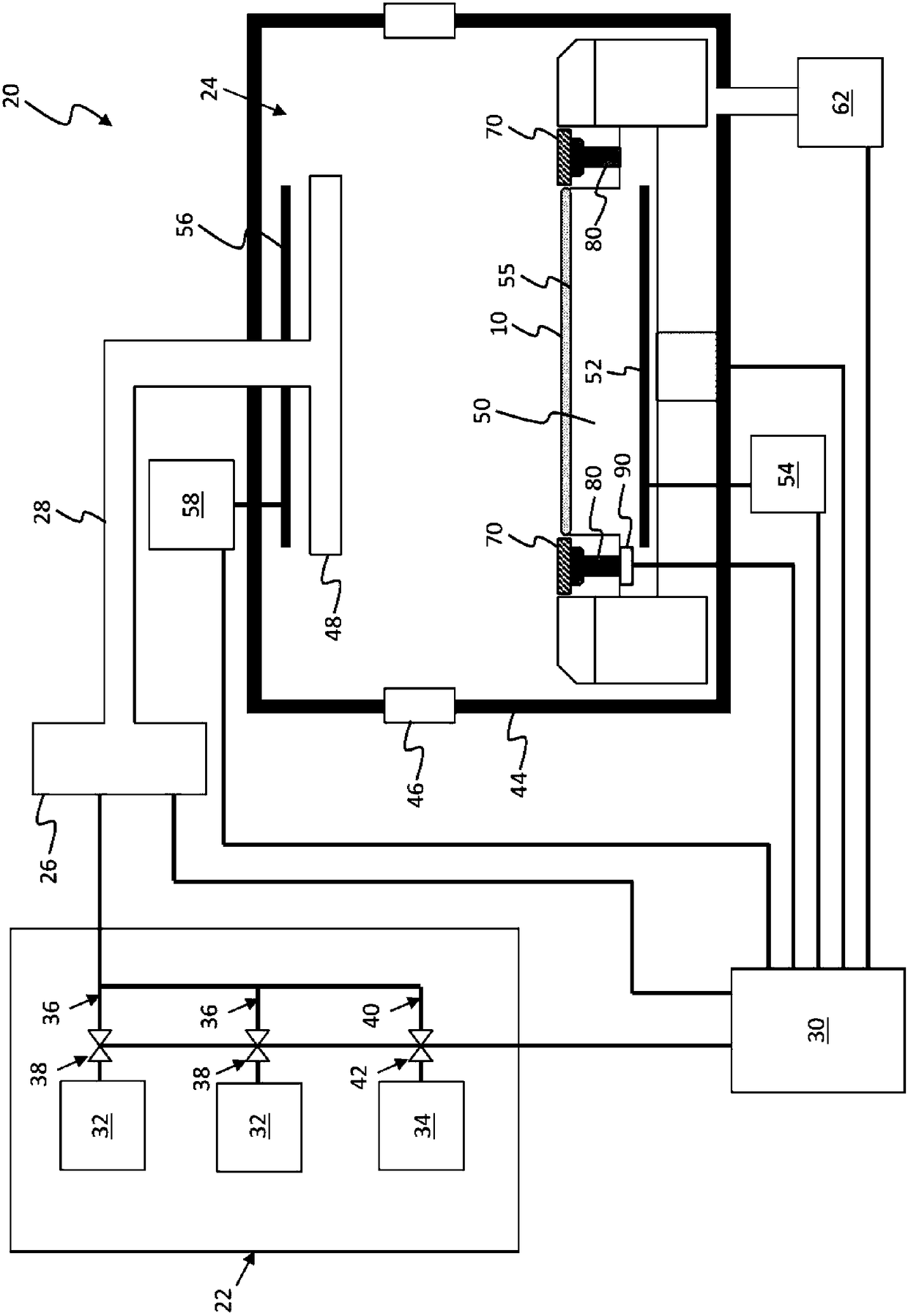
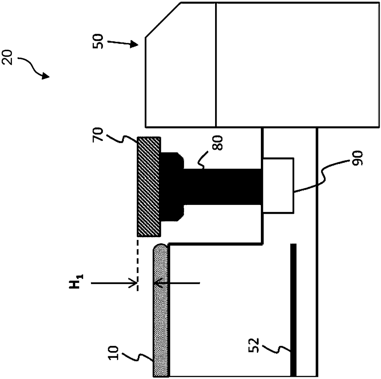
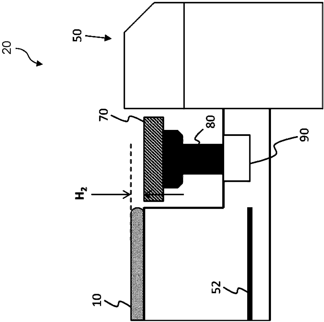
[0054] This specification provides many different embodiments, or examples, for implementing the various features of the invention. Certain components and arrangements are described below only to simplify the description. This is of course only an example and no limitation is intended. For example, in the following description, the formation of the first part on the second part may include embodiments in which the first part is in direct contact with the second part, or embodiments in which other parts are formed between the first part and the second part, Therefore the first part may not be in direct contact with the second part. In addition, this specification may repeat reference numerals and / or letters in various examples, such repetition is for the sake of simplicity and clarity, and does not in itself specify the relationship between the various embodiments and / or structures discussed.

[0055] In addition, spatial relative terms such as "under", "below", "below", "on"...


PUM


Abstract

A semiconductor manufacturing method and a semiconductor manufacturing tool for performing the same are disclosed. The semiconductor manufacturing tool includes a plasma chamber, a mounting platform disposed within the plasma chamber, a focus ring disposed within the plasma chamber, and at least one actuator mechanically coupled to the focus ring and configured to move the focus ring vertically. The actuator is configured to move the focus ring vertically when a plasma is present in the plasma chamber. The provided semiconductor manufacturing method can be used to dynamically control the etching speed of etching process.

Description

technical field [0001] Embodiments of the present invention relate to a semiconductor manufacturing method and device, in particular to a method and device for moving a focus ring in a plasma etching process. Background technique [0002] Semiconductor components are used in various electronic applications, such as personal computers, mobile phones, digital cameras and other electronic equipment. The manufacture of semiconductor devices usually involves depositing insulating or dielectric layers, conductive layers, and semiconductor layer materials on a semiconductor substrate in sequence, and patterning each material layer through lithography and etching processes to form circuit components and units thereon. [0003] The semiconductor industry continues to improve the integration density of electronic components (such as transistors, diodes, resistors and capacitors, etc.) by continuously reducing the minimum feature size to integrate more components into a given area. . ...

Claims


Application Information

Patent Timeline
IPC IPC(8): H01L21/3065
CPCH01L21/3065H01L21/31144H01J37/32642H01J37/32715H01L21/31116H01J2237/334H01L21/67069
Inventor 林育奇林进兴张宏睿邱意为
Owner TAIWAN SEMICON MFG CO LTD
Why Eureka
Try Eureka