Signal control device and control method, display control device and display device

A technology for signal control and display control, applied in the fields of signal control devices and control methods, display control devices, and display devices, which can solve problems such as signal loss, insufficient charging rate of thin-film transistors, and reduced display effect of display panels, so as to improve the opening speed , Improve the display effect and prevent the liquid crystal deflection speed from decreasing

Inactive Publication Date: 2018-06-15
BOE TECH GRP CO LTD +1
View PDF6 Cites 8 Cited by
  • Summary
  • Abstract
  • Description
  • Claims
  • Application Information

AI Technical Summary

Problems solved by technology

[0003] For large-size display panels, the array substrate in the display panel has a large resistance voltage drop, which causes serious loss in the signal transmission process. In this way, when the signal is transmitted to the area of ​​the array substrate far away from the signal terminal, it cannot meet the requirement that the array substrate be far away from the signal terminal. The charging requirements of the area of ​​the signal terminal lead to a serious insufficient charging rate of the thin film transistors contained in the area of ​​the array substrate far away from the signal terminal, thereby reducing the display effect of the display panel

Method used


Image

  • Signal control device and control method, display control device and display device
  • Signal control device and control method, display control device and display device
  • Signal control device and control method, display control device and display device

Examples


Embodiment Construction

[0036] The following will clearly and completely describe the technical solutions in the embodiments of the present invention with reference to the accompanying drawings in the embodiments of the present invention. Obviously, the described embodiments are only some, not all, embodiments of the present invention. Based on the embodiments of the present invention, all other embodiments obtained by persons of ordinary skill in the art without creative efforts fall within the protection scope of the present invention.

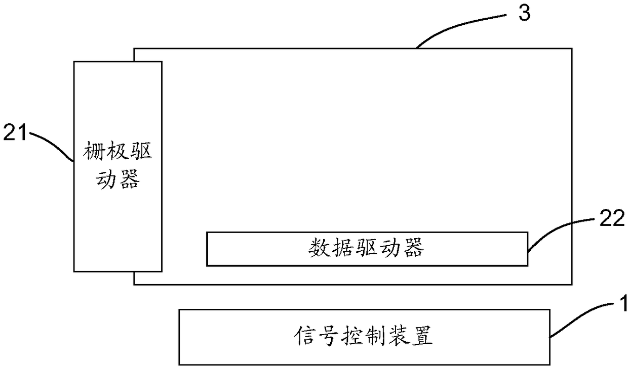
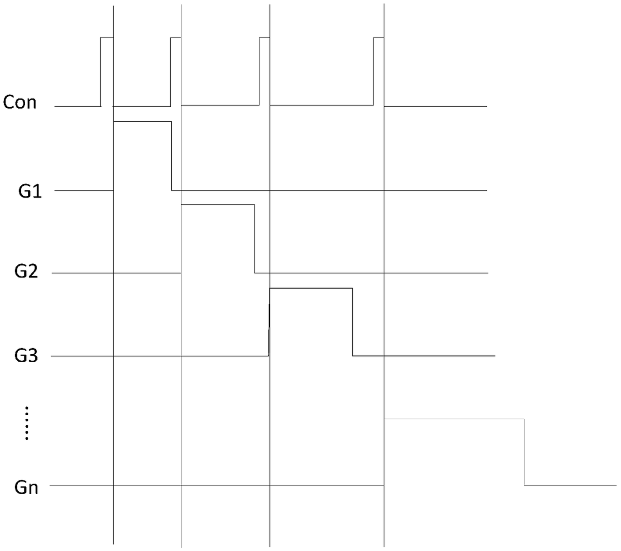
[0037] For large-size display panels in the prior art, the charging rate of the thin film transistors in the area of ​​the display panel far away from the signal terminals is insufficient, such as figure 1 As shown, the embodiment of the present invention provides a signal control device and method, so as to realize the modulation of the timing of the display control signal.

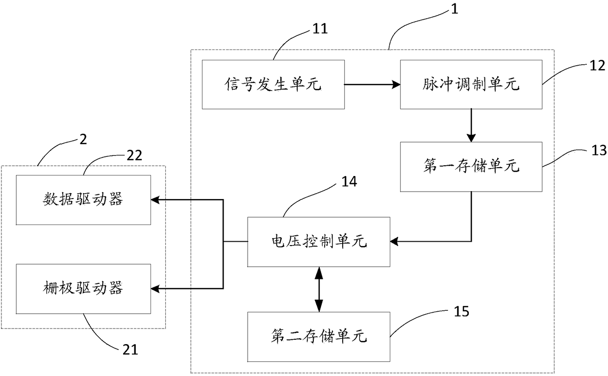
[0038] Such as figure 1 and figure 2 As shown, when the display control device is appl...


PUM


Abstract

The invention discloses a signal control device and a control method, a display control device and a display device and relates to the display technology field. The invention aims at increasing the charging rate of a thin film transistor contained in the area of an array substrate and guaranteeing the display effect of a display panel, wherein the area is far away from a signal terminal. The signal control device comprises a signal generating unit and a pulse modulation unit, wherein the signal generating unit is used for generating an initial enabled control signal; the pulse modulation unitis connected to the signal generating unit and is used for modulating the pulse displacement of the initial enabled control signal so as to acquire a modulated enabled control signal, and in each scanning period, the pulse displacement of the modulated enabled control signal is gradually increased; and the modulated enabled control signal is used for controlling the output timing sequence of display control signals. The display control device comprises the signal control device mentioned in the above technical scheme. The signal control device and the control method, the display control deviceand the display device are used in the display device.

Description

technical field [0001] The present invention relates to the field of display technology, in particular to a signal control device and a control method, a display control device, and a display device. Background technique [0002] When an existing display panel realizes image display, a timing controller is used to send timing signals to control the transmission time of scanning signals and data signals to the display panel, thereby realizing image display on the display panel. [0003] For large-size display panels, the array substrate in the display panel has a large resistance voltage drop, which causes serious loss in the signal transmission process. In this way, when the signal is transmitted to the area of ​​the array substrate far away from the signal terminal, it cannot meet the requirement that the array substrate be far away from the signal terminal. The charging requirements of the area of ​​the signal terminals lead to a serious insufficient charging rate of the t...

Claims


Application Information

Patent Timeline
Patent Type & Authority Applications(China)
IPC IPC(8): G09G3/36
CPCG09G3/3696G09G3/20G09G2310/0267G09G2310/0275G09G2320/0223G09G3/2074G09G3/2011G09G3/2014
Inventor 孔小丽
Owner BOE TECH GRP CO LTD
Why Eureka
Try Eureka