High-resolution display plasma module and manufacturing method thereof

A high-resolution, manufacturing method technology, applied in nonlinear optics, instruments, optics, etc., to achieve the effect of ensuring the directionality and verticality of the electric field, improving the contrast, and displaying better effects

Pending Publication Date: 2018-06-19
WUXI VISION PEAK TECH
View PDF8 Cites 11 Cited by
  • Summary
  • Abstract
  • Description
  • Claims
  • Application Information

AI Technical Summary

Problems solved by technology

[0008] The purpose of the present invention is to provide a high-resolution display plasma module and its manufacturing method for the current problems of electronic display screens, which can directly use the display plasma to replace the existing microcup structure or microcapsules, and in the pixel The electrode is provided with a plasma barrier barrier array located in the gap between the pixel electrode units, and the patterned structure of the plasma barrier barrier array surrounds each pixel electrode unit, thereby obtaining a high-resolution display effect. The display electrode of the present invention Plasma module, can achieve high resolution, multi-color, multi-grayscale display effect

Method used


Image

  • High-resolution display plasma module and manufacturing method thereof
  • High-resolution display plasma module and manufacturing method thereof

Examples


Embodiment Construction

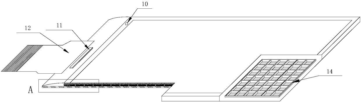
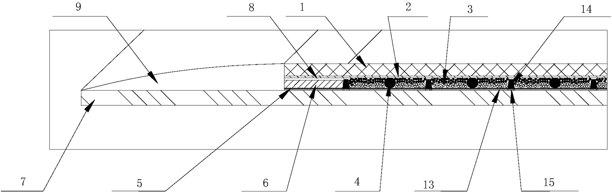
[0040] The present invention will be further described below in conjunction with specific drawings and embodiments.

[0041] The present invention is not limited to the following embodiments, and the figures referred to in the following description are provided for understanding the content of the present invention, that is, the present invention is not limited to the structure of the electronic ink display screen exemplified in each figure.

[0042] as attached figure 1 and figure 2As shown, the embodiment takes a dual-particle electronic ink display screen as an example, a high-resolution display plasma module, including a pixel electrode 13 and a transparent electrode 1 located above the pixel electrode 13, characterized in that the pixel electrode 13 and the transparent electrode 1 are provided with a display plasma 3 and a liner frame 6 located around the display plasma 3, and the pixel electrode 13 is provided with a plasma blocking weir for uniformly dispersing and st...


PUM

PropertyMeasurementUnit
thicknessaaaaaaaaaa
diameteraaaaaaaaaa
widthaaaaaaaaaa

Abstract

The invention belongs to the technical field of electronic display and relates to a high-resolution display plasma module and a manufacturing method thereof. The high-resolution display plasma modulecomprises a pixel electrode and a transparent electrode; a liner frame which is used for displaying plasma and is arranged at the periphery of the plasma is arranged between the pixel electrode and the transparent electrode; the pixel electrode is provided with a plasma isolation weir array; the plasma isolation weir array comprises a plurality of plasma isolation weirs which are distributed in anarray; the pixel electrode comprises a plurality of pixel electrode units which are distributed in the array; and the plasma isolation weirs, each of which contains one pixel electrode unit only, arearranged in intervals among the pixel electrode units respectively. By adopting the high-resolution display plasma module provided by the invention, display plasma is used to replace the existing microcup structure or microcapsule, and the plasma isolation weir array which is of a patterned structure and is arranged in the intervals among the pixel electrode units is arranged on the pixel electrode and encircles the pixel electrode units, so that high-resolution display effect is acquired, and multicolor and multi-gray display effect can be realized.

Description

technical field [0001] The invention relates to a display plasma module and a manufacturing method thereof, in particular to a high-resolution display plasma module and a manufacturing method thereof, belonging to the technical field of electronic display. Background technique [0002] Electrophoretic display utilizes the phenomenon of swimming of charged colloidal particles under the action of an electric field, and drives electrophoretic particles with different photoelectric properties through the electric field to realize the display of images and text. Compared with known display technologies, electrophoretic display has the following characteristics: flexible It is easy to bend, light in weight, thin in thickness, high in contrast, low in energy consumption, wide in viewing angle, readable in sunlight, has image bistable state, and is easy to produce on a large scale. [0003] Electrophoretic display technology was first proposed in the 1970s. Patent US3892568 disclos...

Claims


Application Information

Patent Timeline
Patent Type & Authority Applications(China)
IPC IPC(8): G02F1/167
CPCG02F1/167
Inventor 张磊陈山包进
Owner WUXI VISION PEAK TECH
Why Eureka
Try Eureka