A New Voltage Domain Oscillating Diode

A technology of voltage domain and diode, which is applied in the field of compound semiconductor quantum devices, can solve the problems that are difficult to meet the design and application of traditional multi-valued logic circuits, and the regularity of current oscillation is chaotic.

Active Publication Date: 2021-01-26
SHANGRAO NORMAL UNIV
View PDF3 Cites 0 Cited by
  • Summary
  • Abstract
  • Description
  • Claims
  • Application Information

AI Technical Summary

Problems solved by technology

); when the thickness of the collector barrier is 2nm and the bias voltage is below 1V, the optimally designed GaAs / AlGaAs RTD may have multiple peaks and multiple valleys in some cases. <2.5, difficult to meet the traditional multi-valued logic (MVL) circuit design application, it may be possible to be used in low-voltage low-power pure quantum logic (PQL) circuit design
[0004] The present invention proposes a diode with FKO characteristics——Franz-Keldysh oscillating diode (FKOD); so far, there is no FKOD device in conventional GaAs / AlGaAs, GaN / AlGaN-based diode devices

Method used


Image

  • A New Voltage Domain Oscillating Diode
  • A New Voltage Domain Oscillating Diode
  • A New Voltage Domain Oscillating Diode

Examples


Embodiment Construction

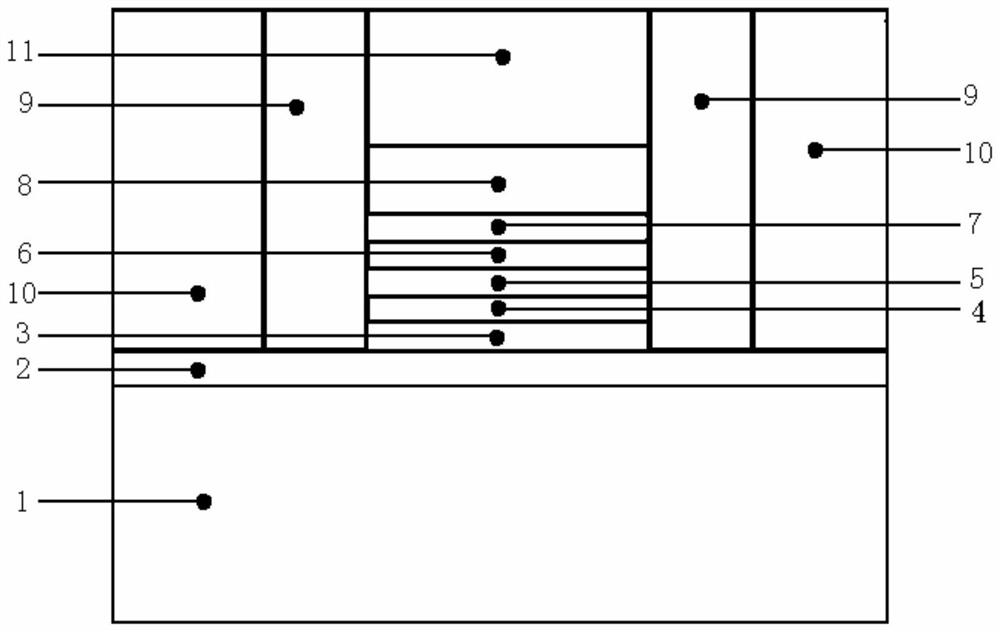
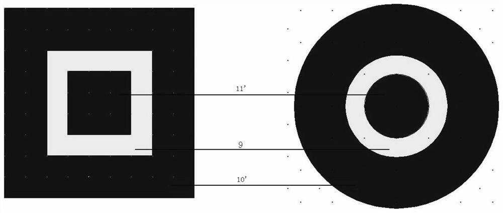
[0029] Such as figure 1 As shown, a new voltage domain oscillator diode, including a substrate 1, a collector layer 2, a first isolation layer 3, a first barrier layer 4, a quantum well layer 5, a second barrier layer 6, a second isolation layer 7. The emitter layer 8, the passivation layer 9, the metal electrode pin 10 in the collector area, and the metal electrode pin 11 in the emitter area. Epitaxial collector region layer 2 on the upper surface of substrate 1, epitaxial first isolation layer 3, first barrier layer 4, quantum well layer 5, second barrier layer 6, and second isolation layer 7 in the middle of the upper surface of collector region layer 2 With the emitter layer 8; the first isolation layer 3, the first barrier layer 4, the quantum well layer 5, the second barrier layer 6, the second isolation layer 7 and the emitter layer 8 constitute the central quantum structure of the resonant tunneling diode area. The upper surface of the central quantum structure area ...


PUM

PropertyMeasurementUnit
thicknessaaaaaaaaaa

Abstract

The invention relates to a novel voltage domain oscillation diode. The present invention includes a GaN substrate whose initial upper surface is a gallium plane, n + ‑qInGaN collector layer, i‑InGaN first isolation layer, i‑InGaN first barrier layer, i‑InGaN quantum well layer, i‑GaN second barrier layer, i‑InGaN second isolation layer, n + ‑InGaN emitter layer, AlN passivation layer, collector metal electrode pins, and emitter metal electrode pins. The present invention adopts the polarized electric field of the barrier layer of the GaN-based double-barrier single-quantum well superlattice structure to weaken the effect of the applied electric field, and effectively suppress the in-band resonant tunneling in the low bias voltage region; utilize the collector area close to the collector barrier The depletion layer acts as the auxiliary potential barrier of the collector barrier, and the volt-ampere characteristics in the higher bias region show multi-coordinated current oscillation, resonance tunneling and superposition of electron wave functions corresponding to each energy level, forming many differential negative resistance regions Aligned with the positive resistance area.

Description

technical field [0001] The invention relates to the technical field of compound semiconductor quantum devices, in particular to a novel voltage domain oscillating diode. Background technique [0002] Double barrier single quantum well heterojunction diodes, due to the influence of external bias and polarization effects, when the diode is at a higher bias voltage (for GaN-based devices, the bias voltage is greater than 2.5V), its quantum well When a non-uniform electric field is formed, in the field of optoelectronics, the optical absorption coefficient and dielectric constant of the device above the band edge (that is, the high-energy region of the energy domain) manifest as amplitude modulation and phase modulation oscillation, that is, the modulation spectrum in the frequency domain is generated. This type of oscillation is called optical Franz-Keldysh oscillation (OFKO). In the field of optoelectronics, low-dimensional semiconductor quantum dots, quantum well structures ...

Claims


Application Information

Patent Timeline
Patent Type & Authority Patents(China)
IPC IPC(8): H01L29/88
CPCH01L29/882
Inventor 张海鹏张强张忠海林弥吕伟锋白建玲
Owner SHANGRAO NORMAL UNIV
Why Eureka
Try Eureka