A Scanning Thermoelectric Microscopy Device for Thermoelectric Figure of Merit Behavioral Microscopic Imaging

A thermoelectric figure of merit and microscopic imaging technology, applied in scanning probe microscopy, scanning probe technology, measuring devices, etc. Promote and apply, test direct, compatible effects

Active Publication Date: 2019-10-18
SHANGHAI INST OF CERAMIC CHEM & TECH CHINESE ACAD OF SCI
View PDF5 Cites 0 Cited by
  • Summary
  • Abstract
  • Description
  • Claims
  • Application Information

AI Technical Summary

Problems solved by technology

So far, there is no high-resolution microscopic imaging technology that can realize the spatial distribution of thermoelectric figure of merit, so it is difficult to intuitively understand and reveal the dynamic laws of micro-region thermoelectric transport

Method used


Image

  • A Scanning Thermoelectric Microscopy Device for Thermoelectric Figure of Merit Behavioral Microscopic Imaging
  • A Scanning Thermoelectric Microscopy Device for Thermoelectric Figure of Merit Behavioral Microscopic Imaging
  • A Scanning Thermoelectric Microscopy Device for Thermoelectric Figure of Merit Behavioral Microscopic Imaging

Examples


Embodiment 1

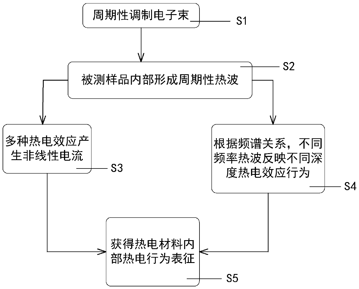
[0117] Using the high-resolution microscopic imaging device for subsurface thermoelectric signals established in this application—electron beam modulation scanning thermoelectric microscope, the subsurface thermoelectric behavior of thermoelectric materials and devices was tested, and the results are as follows: Image 6 with Figure 7 shown.

[0118] Image 6 gave a Bi 2 Te 3 The results of thermoelectric microscopic imaging of bulk thermoelectric materials at different frequencies, where picture (a) is the secondary electron image of the sample surface topography, and picture (b-i) is the double-frequency thermoelectric Seebeck current image of the sample. It can be seen from the figure that the thermoelectric Seebeck current image shows completely different information from the topographic image in figure (a). It is closely related to the strong scattering of thermoelectric transport carriers. The thermoelectric microscopic images of different frequencies reflect the t...

Embodiment 2

[0120] Figure 7 (a) is one Bi 2 Te 3 The results of thermoelectric microscopic imaging of bulk thermoelectric devices, in which picture (a) is the secondary electron image of the surface topography of the thermoelectric device, showing the topography of thermoelectric materials and metal electrodes on the surface of the device, and picture (b) is the picture ( The thermoelectric microscopic image of the boxed area in a) shows that the thermoelectric material shows thermoelectric contrast information, but the metal electrode part of the device does not, which fully illustrates the scanning thermoelectric microscopy of electron beam modulation Contrast comes only from the thermoelectric effect. The complex thermoelectric contrast image of the thermoelectric material in Figure (b) reflects the interaction behavior of the thermoelectric transport carriers in the micro-area of ​​the thermoelectric material and the microstructures such as grains, grain boundaries, and defects in ...


PUM


Abstract

The invention discloses a scanning thermoelectric microscopy device for microimaging of thermoelectric FOM (Figure of Merit) factor behaviors. The device is used for resolution microimaging of sub-surface thermoelectric FOM factor behaviors of a to-be-tested thermoelectric material sample. The device includes a subsurface thermoelectric signal in situ excitation module used for in situ excitationof subsurface thermoelectric Seebeck current signals of the to-be-tested thermoelectric material sample; a thermoelectric signal in situ detection module used for in situ real time detection of the subsurface thermoelectric Seebeck current signals of the to-be-tested thermoelectric material sample; a thermoelectric signal microimaging module used for high resolution microimaging and displaying ofthe subsurface thermoelectric FOM factor signals. The device provided by the invention has unique functions of in situ excitation and in situ synchronous representation of subsurface thermoelectric signals and has advantages of high resolution rate, high flexibility, high signal to noise ratio, testing directness and the like. The device is simple in structure and high in compatibility, is suitable for combination with different commercial scanning electron microscopes and is a novel technique easy to promote and apply.

Description

technical field [0001] The application relates to the field of signal detection instruments, in particular to a scanning pyroelectric microscopy device for pyroelectric figure of merit behavioral microscopic imaging. Background technique [0002] As an important energy material at present, thermoelectric materials based on the mutual conversion effect of heat energy and electric energy are used in many important high-tech industries such as the recycling of industrial waste heat and automobile exhaust heat, high-precision temperature control devices, space technology, military equipment, and information technology. It has a very broad application prospect in the field, which has attracted great attention from all over the world. For example, the United States has developed semiconductor thermoelectric materials to realize high-efficiency space power supplies that convert nuclear reaction heat energy into electrical energy, providing high-efficiency space power for its return ...

Claims


Application Information

Patent Timeline
Patent Type & Authority Patents(China)
IPC IPC(8): G01Q60/58
Inventor 曾华荣徐琨淇赵坤宇陈立东李国荣
Owner SHANGHAI INST OF CERAMIC CHEM & TECH CHINESE ACAD OF SCI
Why Eureka
Try Eureka