Planar illumination device and method of manufacturing planar illumination device

A lighting device and manufacturing method technology, applied in the direction of instruments, nonlinear optics, optics, etc., can solve the problems of deterioration of installation accuracy and inability to obtain brightness characteristics, and achieve the effect of excellent brightness characteristics

Pending Publication Date: 2018-06-29
MINEBEA CO LTD
View PDF8 Cites 2 Cited by
  • Summary
  • Abstract
  • Description
  • Claims
  • Application Information

AI Technical Summary

Problems solved by technology

[0006] However, in the prior art as described above, since the self-calibration works, the mounting accuracy of the LEDs deteriorates instead, and thus sufficient luminance characteristics cannot be obtained in some cases.

Method used


Image

  • Planar illumination device and method of manufacturing planar illumination device
  • Planar illumination device and method of manufacturing planar illumination device
  • Planar illumination device and method of manufacturing planar illumination device

Examples


Embodiment Construction

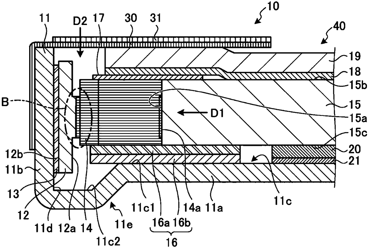
[0029] Next, the planar lighting device and the manufacturing method according to the embodiment will be described with reference to the drawings. In addition, the dimensional relationship of each element in the drawings, the ratio of each element, and the like may differ from reality. Even among the drawings, there may be a part where the mutual dimensional relationship and ratio are different.

[0030]

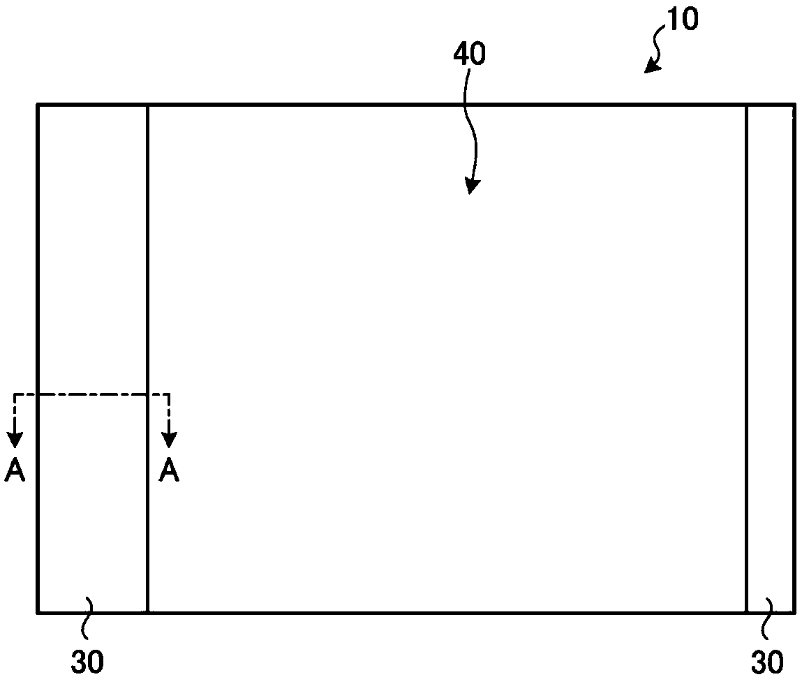
[0031] first use figure 1 The outline of the planar lighting device 10 will be described. figure 1 It is a top view showing an example of the appearance of the planar lighting device 10 according to the embodiment. Such as figure 1 As shown, the planar lighting device 10 according to the embodiment emits light from the effective region 40 which is an emission region not covered by the light-shielding sheet 30 . That is, the effective area 40 is defined by the light shielding sheet 30 .

[0032] The planar lighting device 10 according to the embodiment is used as a bac...


PUM


Abstract

The invention provides a planar illumination device and a method of manufacturing the planar illumination device, which meets the requirement for thinness and obtains excellent brightness features. Aplanar illumination device according to an embodiment includes a light guide plate, a light source, a substrate, and a fixing member. The light guide plate causes light incident on a side surface to exit from a light exit surface. The light source is arranged on a side of the side surface of the light guide plate and has a light emitting surface to emit light toward the side surface. The light source is mounted on the substrate by bonding a bonding surface of the light source thereto by a solder. The fixing member is cured at temperature lower than a melting point of the solder and fixes the light source to the substrate while maintaining a position and a posture of the light source.

Description

technical field [0001] The present invention relates to a planar lighting device and a method for manufacturing the planar lighting device. Background technique [0002] There is a planar lighting device in which LEDs mounted on a substrate via solder, such as top-emission and side-emission LEDs (Light Emitting Diodes), are arranged to face the light-incident surface of a light guide plate. [0003] Conventionally, when soldering LEDs, there is known a technique of correcting misalignment and inclination (posture change) of LEDs caused by melting of solder by self-calibration. [0004] Patent Document 1: Japanese Patent Application Laid-Open No. 8-130363 [0005] In recent years, light guide plates have become relatively thin compared to the thickness of top-emission LEDs in response to demands for narrower frames of planar lighting devices. In order to obtain sufficient luminance characteristics even in such a situation, it is necessary to align the LED and the light guid...

Claims


Application Information

Patent Timeline
Patent Type & Authority Applications(China)
IPC IPC(8): G02F1/13357
CPCG02F1/133615
Inventor 田中一弘下出智久枝光贵志
Owner MINEBEA CO LTD
Why Eureka
Try Eureka