Fingerprint identification detection circuit and touch control panel

A detection circuit and fingerprint recognition technology, which is applied in character and pattern recognition, acquisition/organization of fingerprints/palmprints, instruments, etc., can solve the problems of large space on the backplane and cannot be integrated, and achieve the effect of saving space

Active Publication Date: 2018-06-29
BOE TECH GRP CO LTD
View PDF4 Cites 10 Cited by
  • Summary
  • Abstract
  • Description
  • Claims
  • Application Information

AI Technical Summary

Problems solved by technology

However, since the active detection circuit contains at least three or more thin-film transistors (TFTs), when facing a high-resolution (PPI) screen, it will encounter the problem of occupying too much space on the backplane and cannot be integrated.

Method used


Image

  • Fingerprint identification detection circuit and touch control panel
  • Fingerprint identification detection circuit and touch control panel
  • Fingerprint identification detection circuit and touch control panel

Examples


Embodiment 1

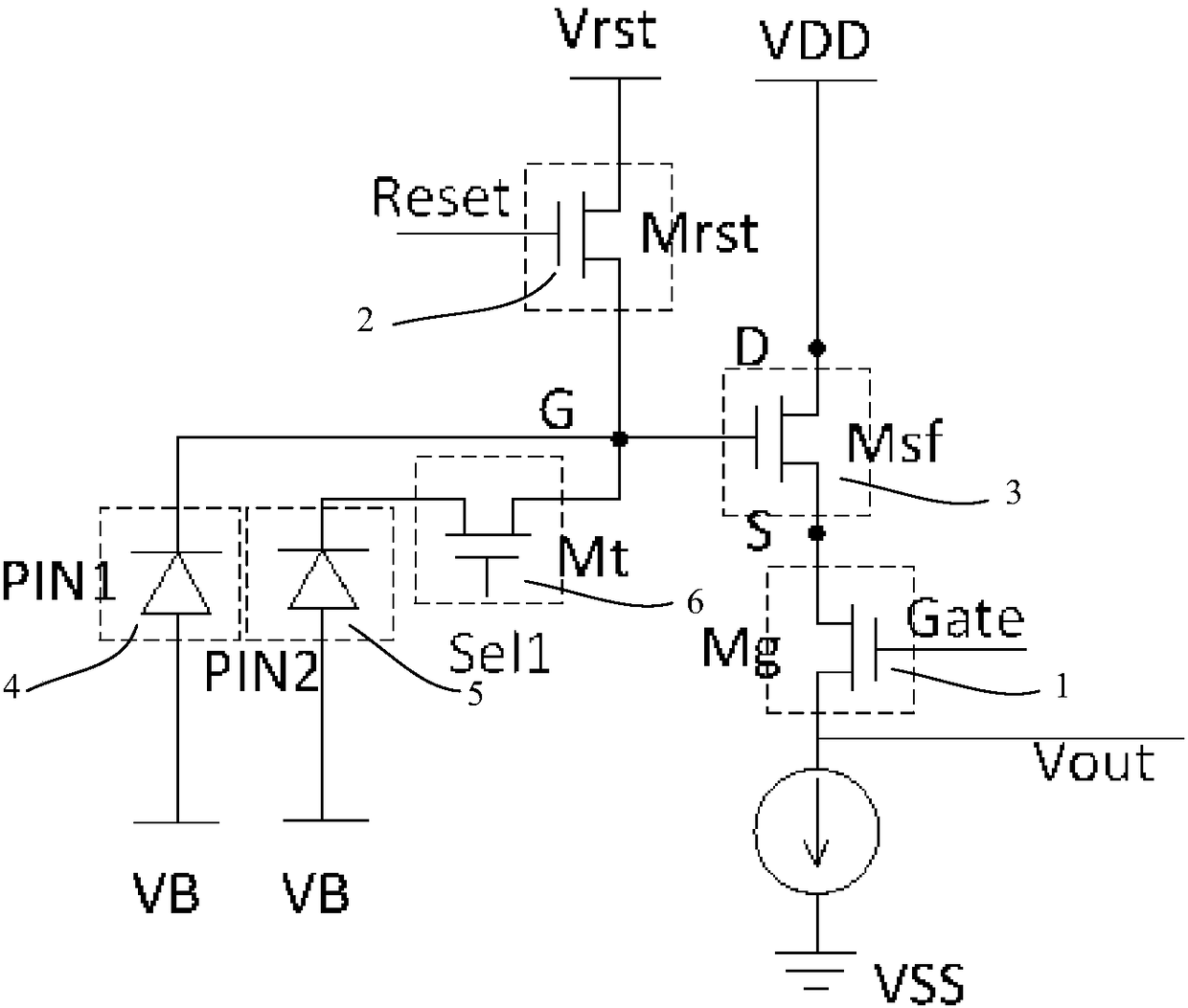
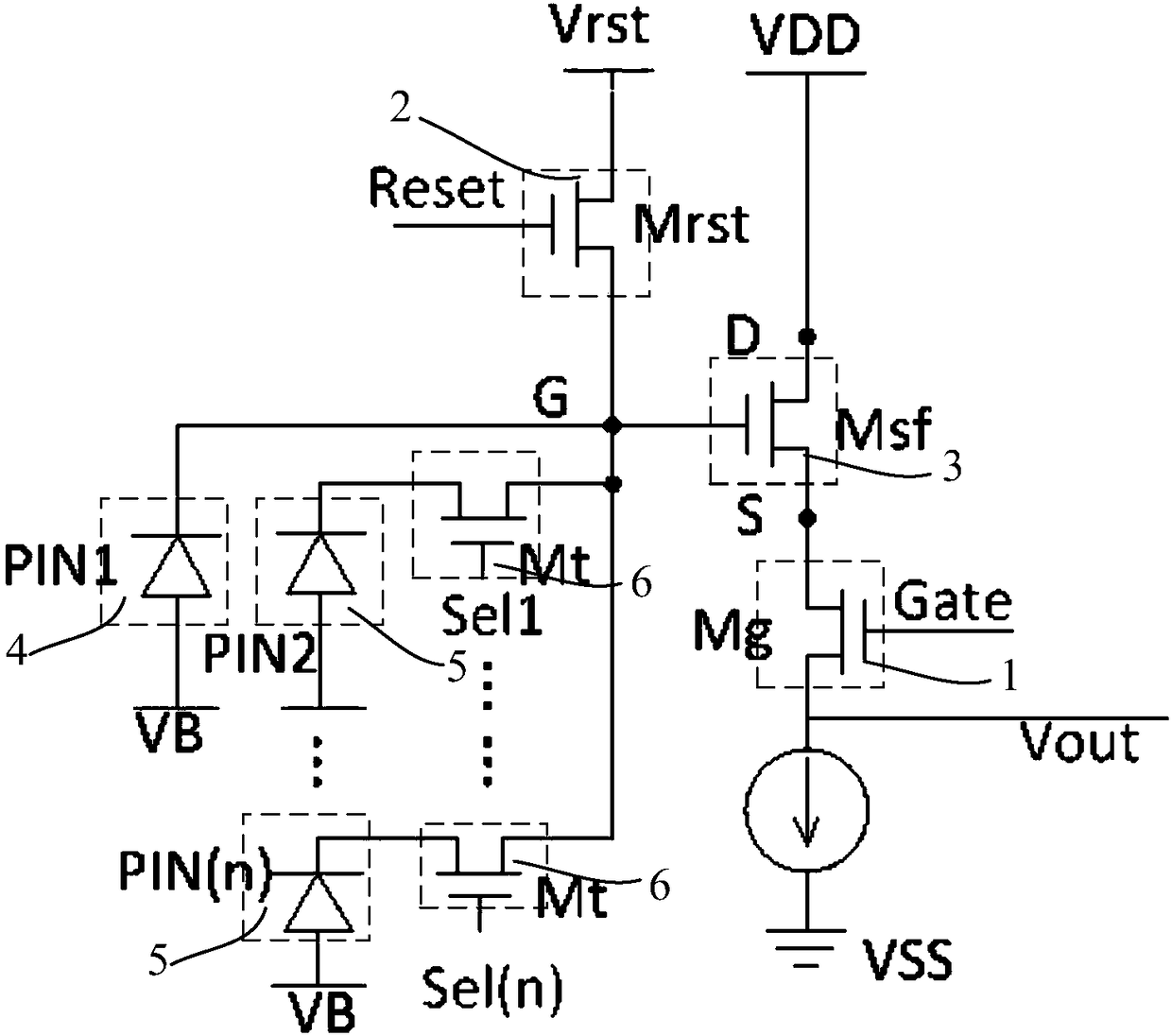
[0032] combine Figure 1-3 As shown, this embodiment provides a fingerprint recognition detection circuit, reset unit 2, current generating unit 3, switch unit 1, first photosensitive unit 4, at least one second photosensitive unit 5, and at least each second photosensitive unit 5 The current generation unit 3 is connected to the corresponding selection unit 6 respectively; wherein, the reset unit 2 is used to reset the first photosensitive unit 4 and each second photosensitive unit 5 through the initialization voltage under the control of the reset signal; Both the first photosensitive unit 4 and the second photosensitive unit 5 are used to generate corresponding electrical signals according to the sensed light signals; The electrical signal is transmitted to the current generation unit 3; the current generation unit 3 is used to generate a corresponding leakage current according to the received electrical signal; the switch unit 1 is used to output the leakage current output ...

Embodiment 2

[0061] This embodiment provides a touch panel, which includes the fingerprint recognition and detection circuit in Embodiment 1, that is, each fingerprint recognition and detection circuit includes a first photosensitive unit 4 and at least one second photosensitive unit 5, that is, includes a A plurality of photosensitive units, and a plurality of photosensitive units share the reset unit 2, the current generating unit 3, and the switch unit 1, therefore, the fingerprint detection circuit can measure the light signals induced by the plurality of photosensitive units to realize fingerprint identification, so that the When the fingerprint identification and detection circuit is formed in the touch panel, the space is greatly saved, and thus the touch panel can realize a high-resolution design.

[0062] Wherein, the touch panel includes a plurality of pixel units; wherein, the first light-sensing unit 4 and each second light-sensing unit 5 in each fingerprint recognition detectio...


PUM


Abstract

The present invention provides a fingerprint identification detection circuit and a touch control panel, belonging to the technical field of display. The fingerprint identification detection circuit comprises: a reset unit configured to perform reset of a first photosensitive unit and each second photosensitive unit through adoption of an initialization voltage under the control of reset signals;the first photosensitive unit and the second photosensitive units configured to generate corresponding electrical signals according to the inducted optical signals; a selection unit configured to transmit the electrical signals generated by the second photosensitive units to a current generation unit under the control of the selection signals; the current generation unit configured to generate a corresponding leak current according to the received electrical signals; and a switch unit configured to output the leak current output by the current generation unit under the control of scanning signals for identification of fingerprint information.

Description

technical field [0001] The invention belongs to the field of display technology, and in particular relates to a fingerprint identification detection circuit and a touch panel. Background technique [0002] The current fingerprint identification devices are capacitive and ultrasonic, each has its advantages and disadvantages, but there is a common defect that the fingerprint identification device has a short sensing distance, which severely limits the structure and performance of the fingerprint identification device and affects its application in mobile terminals. Wide application in products. [0003] Due to the use of optical methods, optical fingerprint recognition naturally has the advantage of long-distance sensing, but due to the high-resolution requirements of optical fingerprint recognition devices, it can only be done very small, and because the signal volume is usually different from that of fingerprint recognition devices. If the area is proportional, then the si...

Claims


Application Information

Patent Timeline
Patent Type & Authority Applications(China)
IPC IPC(8): G06K9/00
CPCG06V40/1318
Inventor 王鹏鹏王海生丁小梁郑智仁韩艳玲刘伟曹学友张平
Owner BOE TECH GRP CO LTD
Why Eureka
Try Eureka