Integrated circuit chip binding structure, preparation method thereof and display device

A technology for integrated circuits and display devices, which is applied in static indicators, instruments, nonlinear optics, etc., and can solve the problem of uneven stress on the integrated circuit chip binding structure, cracks in the integrated circuit chip binding structure, and conductive bumps that cannot be electrically contact, etc.

Pending Publication Date: 2018-07-13
BOE TECH GRP CO LTD +1
View PDF4 Cites 7 Cited by
  • Summary
  • Abstract
  • Description
  • Claims
  • Application Information

AI Technical Summary

Problems solved by technology

[0006] Embodiments of the present invention provide an integrated circuit chip binding structure, its preparation method, and a display device, which can improve the binding process of the prior art due to the fact that the integrated circuit chip binding structure cannot be flatly bonded...

Method used


Image

  • Integrated circuit chip binding structure, preparation method thereof and display device
  • Integrated circuit chip binding structure, preparation method thereof and display device
  • Integrated circuit chip binding structure, preparation method thereof and display device

Examples


Embodiment Construction

[0032] The following will clearly and completely describe the technical solutions in the embodiments of the present invention with reference to the accompanying drawings in the embodiments of the present invention. Obviously, the described embodiments are only some, not all, embodiments of the present invention. Based on the embodiments of the present invention, all other embodiments obtained by persons of ordinary skill in the art without making creative efforts belong to the protection scope of the present invention.

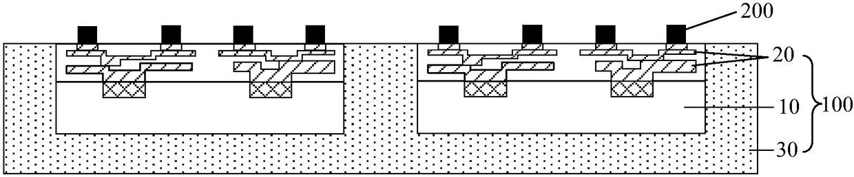
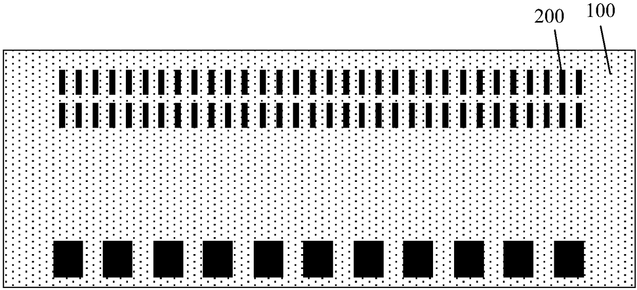
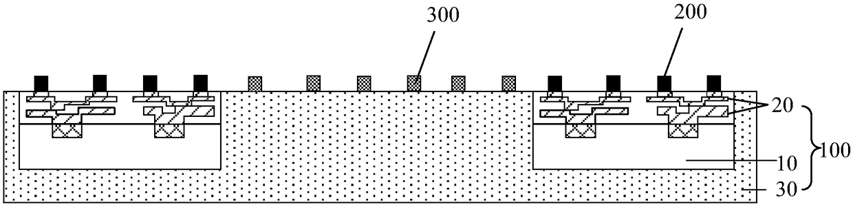
[0033] An embodiment of the present invention provides an integrated circuit chip bonding structure, such as image 3 As shown, it includes a base 100 and a plurality of conductive bumps 200 disposed on the base 100, and the conductive bumps 200 are electrically connected to the chip 10 in the base 100; as Figure 4 As shown, the substrate 100 includes a first region 110 and a second region 120 disposed on the periphery of the first region 110, and the conduct...


PUM


Abstract

The invention provides an integrated circuit chip binding structure, a preparation method thereof and a display device, and relates to the technical field of display. The structure can improve the problems that an integrated circuit chip binding structure cannot be flatly fitted with a substrate in the binding process, so that stress of the integrated circuit chip binding structure is uniform, andfurther, a conductive bump cannot stably and electrically contact with other devices or the integrated circuit chip binding structure is cracked in the prior art. The integrated circuit chip bindingstructure comprises a base, a plurality of conductive bumps and at least one supporting bump, the conductive bumps are arranged on the base and electrically connected with a chip in the base, the basecomprises a first area and a second area arranged on the periphery of the first area, the conductive bumps are arranged on the second area, and the supporting bumps are arranged on the base and arranged in the first area.

Description

technical field [0001] The invention relates to the field of display technology, in particular to an integrated circuit chip binding structure, a preparation method thereof, and a display device. Background technique [0002] With the continuous development of display technology, large-sized display devices, such as liquid crystal displays, LCD TVs, and flat panel displays, and small and medium-sized electronic products such as mobile phones, digital cameras, etc., are mainly developed based on lightness, thinness, shortness, and smallness. The trend is to improve the comfort of use and facilitate portability. Under this development trend, it is required that the integrated circuit chip bonding structure in the display module has a high density and a small volume, and while connecting and transmitting input signals and output signals, it minimizes the occupation of the overall space of the display device. [0003] Integrated circuit chip bonding structure in the prior art, ...

Claims


Application Information

Patent Timeline
IPC IPC(8): G02F1/133
CPCG02F1/133
Inventor 王本莲王杨
Owner BOE TECH GRP CO LTD
Why Eureka
Try Eureka