Electrostatic protection method for semiconductor device and semiconductor device

An electrostatic protection and semiconductor technology, applied in the field of electrostatic protection methods and semiconductor devices, can solve problems such as increasing cost, and achieve the effects of reducing body terminal resistance, improving ESD protection capability, and inhibiting parasitic NPN from turning on.

Active Publication Date: 2021-03-19
JOULWATT TECH INC LTD
View PDF5 Cites 0 Cited by
  • Summary
  • Abstract
  • Description
  • Claims
  • Application Information

AI Technical Summary

Problems solved by technology

For double-diffused transistors, the ESD protection capability is generally improved by enlarging the total width of the double-diffused transistors, but this technical solution greatly increases the cost

Method used


Image

  • Electrostatic protection method for semiconductor device and semiconductor device
  • Electrostatic protection method for semiconductor device and semiconductor device
  • Electrostatic protection method for semiconductor device and semiconductor device

Examples


Embodiment Construction

[0025] Preferred embodiments of the present invention will be described in detail below with reference to the accompanying drawings, but the present invention is not limited to these embodiments. The present invention covers any alternatives, modifications, equivalent methods and schemes made within the spirit and scope of the present invention.

[0026] In order to provide the public with a thorough understanding of the present invention, specific details are set forth in the following preferred embodiments of the present invention, but those skilled in the art can fully understand the present invention without the description of these details.

[0027] In the following paragraphs the invention is described more specifically by way of example with reference to the accompanying drawings. It should be noted that all the drawings are in simplified form and use inaccurate scales, which are only used to facilitate and clearly assist the purpose of illustrating the embodiments of t...


PUM


Abstract

The invention discloses an electro-static protection method of a semiconductor device, and a semiconductor device. A substrate is provided with a P-shaped trap area. A first active area is formed in the P-shaped trap area through N+ injecting, and the first active area is leaded out with a source end. A plurality of second active areas are formed in the P-shaped trap area through P+ segmentation injecting. The second active area is leaded out with a body end. The second active area is arranged in the first active area, and the leading-out of the source end occurs after the leading-out of the body end. The invention is advantageous in that the leading-out resistance of the body end can be reduced, and the leading-out resistance of the source end can be increased; the parasitic NPN launchingcan be inhibited, and the ESD protection capability of the semiconductor device can be enhanced.

Description

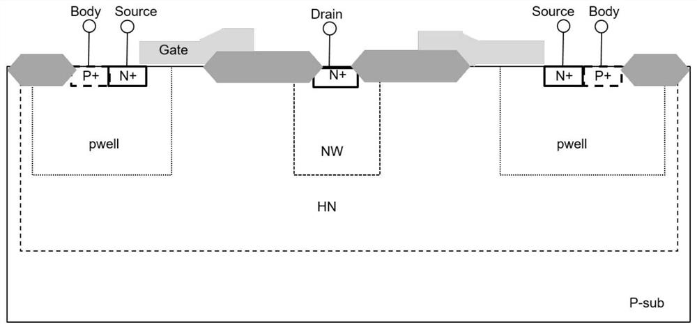
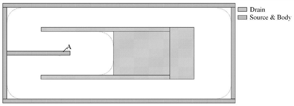
technical field [0001] The invention relates to the technical field of electronic devices, in particular to an electrostatic protection method for a semiconductor device and the semiconductor device. Background technique [0002] ESD (Electrostatic Discharge) is an objective natural phenomenon that accompanies the entire cycle of a product. From the manufacturing, packaging, testing to the application stage of the chip, its external environment and internal structure will accumulate a certain amount of charge, and will be threatened by static electricity at any time. Taking the double-diffused transistor as an example, after the ESD protection is triggered, it often turns on unevenly, causing it to be burned immediately after being triggered, so its self-protection ability is poor. [0003] Such as figure 1 Shown is a schematic cross-sectional view of a double-diffused transistor in the prior art, figure 2 for figure 1 The simple layout of the double-diffused transistor...

Claims


Application Information

Patent Timeline
Patent Type & Authority Patents(China)
IPC IPC(8): H01L27/02
CPCH01L27/0292H01L27/0296
Inventor 韩广涛陆阳周逊伟
Owner JOULWATT TECH INC LTD
Why Eureka
Try Eureka